


Part Number: AM62P
Other Parts Discussed in Thread: , SYSCONFIG, AM623, AM625
Hi,
I am trying to run DDR tests on our custom AM62P board, which has an MT53E1G32D2FW-046 WT:B LPDDR RAM, similar to the one in the SK-AM62P-LP EVM.
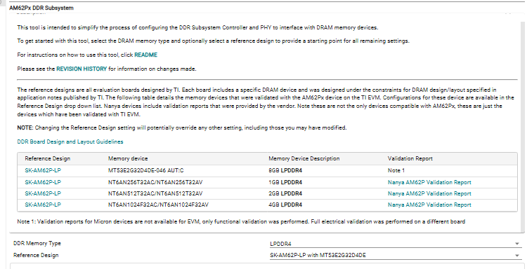
In the DDR SysConfig Tool (https://dev.ti.com/sysconfig/), I created a new project, and configured as follows:
- Software Product: DDR Configuration for AM64x, AM625, AM623, AM62Ax, AM62Px, AM62Dx, AM62Lx (0.10.40)
- Device: AM62P
- Package: FCBGA (AMH)
- Variant: AM62P54 Quad Core A53, Features M. Base features, plus Multimedia JPEG Encoder and Display Subsystem
Then I modified these settings:
- Reference design: SK-AM62P-LP with MT53E2G32D4DE
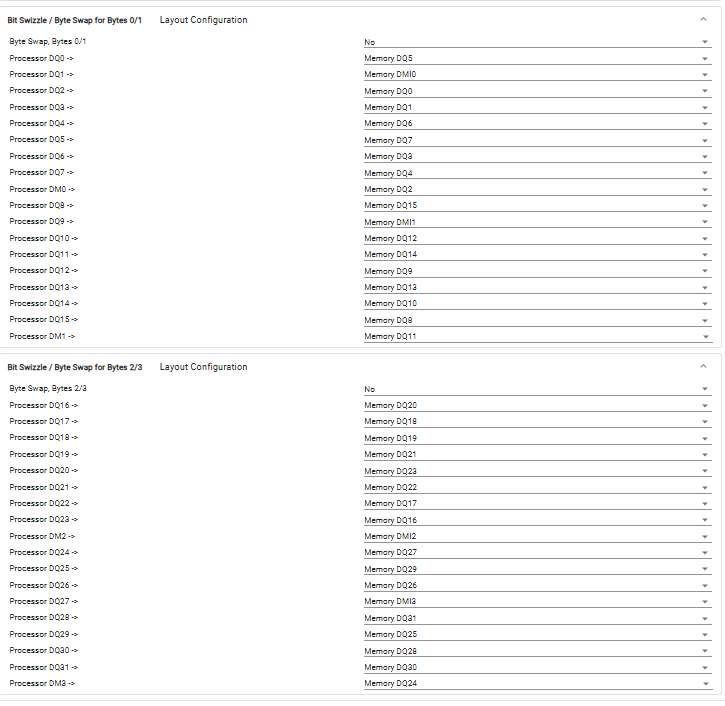
- Bit Swizzle / Byte Swap for Bytes 0/1
- Bit Swizzle / Byte Swap for Bytes 2/3
I changed the Bit Swizzle settings according to our schematics.
After making this configuration, I downloaded the GEL file, and pasted it into:
C:\ti\ccs2051\ccs\ccs_base\emulation\gel\AM62P\AM62P_DDRSS\AM62Px-DDRConfig_Custom.gel
and edited the AM62P_SK_EVM.gel file:StartUp(){ ... GEL_LoadGel("$(GEL_file_dir)/../AM62P_PLL/AM62P_PLL_OFC1.gel");
// Add this line GEL_LoadGel("$(GEL_file_dir)/AM62Px-DDRConfig.gel"); DDR_MODE = LPDDR4;}
I also fixed the top GEL file by adding a delay, as described in this post: AM62P: AM62P DDR test: DDR Basic read/write test Failed - Arm-based microcontrollers forum - Arm-based microcontrollers - TI E2E support forums
C:/ti/ccs2051/ccs/ccs_base/emulation/gel/AM62P/AM62P_DDRSS/AM62P_ddr_top.gel
printf("Clearing the ack bit...\n");
HW_WR_REG32((WKUP_CTRL_MMR0_CFG0_BASE + DDR4_FSP_CLKCHNG_ACK), 0x0); //clear the ack bit // Add this line us_delay(3000); }
printf("--->>> Frequency Change request handshake is completed... <<<---\n");}
Then, I have successfully done the steps described in this post: AM62P: AM62P DDR tests: Error -1170 @ 0x0 Unable to access the DAP. - Arm-based microcontrollers forum - Arm-based microcontrollers - TI E2E support forums
I am able to connect to the board with the XDS110 Debug probe using JTAG, and I can see the DDR test scripts.
The custom GEL file has loaded properly:
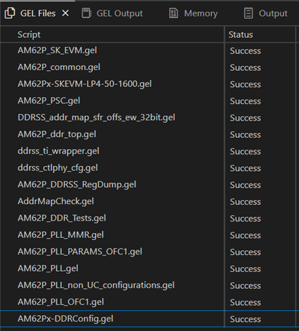
I can successfully run Scripts -> AM62 DDR Initialization -> AM62P_DDR_Initialization_ECC_Disabled.
However, when I try to run Scripts > AM62P DDRSS Memory Debug > Data Tests > Data_WrRd_test, I get:
!!!!! DDR Basic read/write test Failed !!!!
Here is the full GEL output:
WKUP_R5FSS0: ***WARNING: Please close all Memory Browser Windows before attempting to initialize DDR with GELsWKUP_R5FSS0: Running from R5WKUP_R5FSS0:
DDR not initialized with R5 connect.
Go to menu Scripts --> AM62 DDR Initialization -> AM62P_DDR_Initialization_ECC_Disabled to initialize DDR.
====
WKUP_R5FSS0: --->>> ECC Disabled! <<<---WKUP_R5FSS0: --->>> LPDDR4 Initialization is in progress ... <<<---WKUP_R5FSS0: --->>> DDR controller programming in progress.. <<<---WKUP_R5FSS0: --->>> DDR controller programming completed... <<<---WKUP_R5FSS0: --->>> DDR PI programming in progress.. <<<---WKUP_R5FSS0: --->>> DDR PI programming completed... <<<---WKUP_R5FSS0: --->>> Set PHY registers for all FSPs simultaneously (multicast)... <<<---WKUP_R5FSS0: --->>> DDR PHY Data Slice 0 programming in progress.. <<<---WKUP_R5FSS0: --->>> DDR PHY Data Slice 0 programming completed... <<<---WKUP_R5FSS0: --->>> DDR PHY Data Slice 1 programming in progress.. <<<---WKUP_R5FSS0: --->>> DDR PHY Data Slice 1 programming completed... <<<---WKUP_R5FSS0: --->>> DDR PHY Data Slice 2 programming in progress.. <<<---WKUP_R5FSS0: --->>> DDR PHY Data Slice 2 programming completed... <<<---WKUP_R5FSS0: --->>> DDR PHY Data Slice 3 programming in progress.. <<<---WKUP_R5FSS0: --->>> DDR PHY Data Slice 3 programming completed... <<<---WKUP_R5FSS0: --->>> DDR PHY Address Slice 0 programming in progress.. <<<---WKUP_R5FSS0: --->>> DDR PHY Address Slice 0 programming completed... <<<---WKUP_R5FSS0: --->>> DDR PHY Address Slice 1 programming in progress.. <<<---WKUP_R5FSS0: --->>> DDR PHY Address Slice 1 programming completed... <<<---WKUP_R5FSS0: --->>> DDR PHY Address slice 2 programming in progress.. <<<---WKUP_R5FSS0: --->>> DDR PHY Address Slice 2 programming completed... <<<---WKUP_R5FSS0: --->>> DDR PHY programming in progress.. <<<---WKUP_R5FSS0: --->>> DDR PHY programming completed... <<<---WKUP_R5FSS0: Running from R5 or A53WKUP_R5FSS0: Setting MAIN_PLL12_HSDIV0_CLKOUT_25MHzWKUP_R5FSS0: Setting PLL in integer modeWKUP_R5FSS0: Waiting for Calibration Lock...WKUP_R5FSS0: Cal lockedWKUP_R5FSS0: Waiting for PLL Lock...WKUP_R5FSS0: PLL is locked.WKUP_R5FSS0: MAIN_PLL12_HSDIV0_CLKOUT set.WKUP_R5FSS0: --->>> Set DDR to 25MHz for FSP F0... <<<---WKUP_R5FSS0: --->>> DDR PI initialization started... <<<---WKUP_R5FSS0: --->>> DDR CTL initialization started... <<<---WKUP_R5FSS0: --->>> Inside DDR_Change_freq_ack function ... <<<---WKUP_R5FSS0: --->>> Waiting for first frequency change request ... <<<---WKUP_R5FSS0: Waiting for clock change request... WKUP_R5FSS0: Iter 1: Frequency change request type 2 received from controller WKUP_R5FSS0: Running from R5 or A53WKUP_R5FSS0: Setting MAIN_PLL12_HSDIV0_CLKOUT_800MHzWKUP_R5FSS0: Setting PLL in integer modeWKUP_R5FSS0: Waiting for Calibration Lock...WKUP_R5FSS0: Cal lockedWKUP_R5FSS0: Waiting for PLL Lock...WKUP_R5FSS0: PLL is locked.WKUP_R5FSS0: MAIN_PLL12_HSDIV0_CLKOUT set.WKUP_R5FSS0: Setting the FSP ack bit...WKUP_R5FSS0: Waiting for the request to go away...WKUP_R5FSS0: Clearing the ack bit...WKUP_R5FSS0: Waiting for clock change request... WKUP_R5FSS0: Iter 2: Frequency change request type 0 received from controller WKUP_R5FSS0: Running from R5 or A53WKUP_R5FSS0: Setting MAIN_PLL12_HSDIV0_CLKOUT_25MHzWKUP_R5FSS0: Setting PLL in integer modeWKUP_R5FSS0: Waiting for Calibration Lock...WKUP_R5FSS0: Cal lockedWKUP_R5FSS0: Waiting for PLL Lock...WKUP_R5FSS0: PLL is locked.WKUP_R5FSS0: MAIN_PLL12_HSDIV0_CLKOUT set.WKUP_R5FSS0: Setting the FSP ack bit...WKUP_R5FSS0: Waiting for the request to go away...WKUP_R5FSS0: Clearing the ack bit...WKUP_R5FSS0: Waiting for clock change request... WKUP_R5FSS0: Iter 3: Frequency change request type 2 received from controller WKUP_R5FSS0: Running from R5 or A53WKUP_R5FSS0: Setting MAIN_PLL12_HSDIV0_CLKOUT_800MHzWKUP_R5FSS0: Setting PLL in integer modeWKUP_R5FSS0: Waiting for Calibration Lock...WKUP_R5FSS0: Cal lockedWKUP_R5FSS0: Waiting for PLL Lock...WKUP_R5FSS0: PLL is locked.WKUP_R5FSS0: MAIN_PLL12_HSDIV0_CLKOUT set.WKUP_R5FSS0: Setting the FSP ack bit...WKUP_R5FSS0: Waiting for the request to go away...WKUP_R5FSS0: Clearing the ack bit...WKUP_R5FSS0: Waiting for clock change request... WKUP_R5FSS0: Iter 4: Frequency change request type 0 received from controller WKUP_R5FSS0: Running from R5 or A53WKUP_R5FSS0: Setting MAIN_PLL12_HSDIV0_CLKOUT_25MHzWKUP_R5FSS0: Setting PLL in integer modeWKUP_R5FSS0: Waiting for Calibration Lock...WKUP_R5FSS0: Cal lockedWKUP_R5FSS0: Waiting for PLL Lock...WKUP_R5FSS0: PLL is locked.WKUP_R5FSS0: MAIN_PLL12_HSDIV0_CLKOUT set.WKUP_R5FSS0: Setting the FSP ack bit...WKUP_R5FSS0: Waiting for the request to go away...WKUP_R5FSS0: Clearing the ack bit...WKUP_R5FSS0: Waiting for clock change request... WKUP_R5FSS0: Iter 5: Frequency change request type 2 received from controller WKUP_R5FSS0: Running from R5 or A53WKUP_R5FSS0: Setting MAIN_PLL12_HSDIV0_CLKOUT_800MHzWKUP_R5FSS0: Setting PLL in integer modeWKUP_R5FSS0: Waiting for Calibration Lock...WKUP_R5FSS0: Cal lockedWKUP_R5FSS0: Waiting for PLL Lock...WKUP_R5FSS0: PLL is locked.WKUP_R5FSS0: MAIN_PLL12_HSDIV0_CLKOUT set.WKUP_R5FSS0: Setting the FSP ack bit...WKUP_R5FSS0: Waiting for the request to go away...WKUP_R5FSS0: Clearing the ack bit...WKUP_R5FSS0: --->>> Frequency Change request handshake is completed... <<<---WKUP_R5FSS0: pi_int_status = 0x27C02001...WKUP_R5FSS0: - PI_INIT_DONE_BIT set: The power-on initialization training in PI has been completed.WKUP_R5FSS0: - PI_LVL_DONE_BIT set: The leveling operation has completed.WKUP_R5FSS0: - PI_RDLVL_GATE_DONE_BIT set: A read leveling gate training operation has been completed.WKUP_R5FSS0: - PI_RDLVL_DONE_BIT set: A read leveling operation has been completed.WKUP_R5FSS0: - PI_WRLVL_DONE_BIT set: A write leveling operation has been completed.WKUP_R5FSS0: - PI_CALVL_DONE_BIT set: A CA training operation has been completed.WKUP_R5FSS0: - PI_WDQLVL_DONE_BIT set: A write DQ training operation has been completed.WKUP_R5FSS0: - Not documented bit set.WKUP_R5FSS0: ctl_int_status = 0x80002400...WKUP_R5FSS0: --->>> DDR Initialization completed... <<<---WKUP_R5FSS0: --->>> LPDDR4 Initialization is DONE! <<<---WKUP_R5FSS0: Starting WrRd Test 1: *wr32_ptr=i WKUP_R5FSS0: Data verification failed at 0x80000000 Expected = 0x00000000 Actual= 0x00000000WKUP_R5FSS0: Data verification failed at 0x80000004 Expected = 0x01010101 Actual= 0x00000000WKUP_R5FSS0: Starting WrRd Test 2: *wr32_ptr=~i WKUP_R5FSS0: Data verification failed at 0x80000000 Expected = 0x030100FF Actual= 0x00000000WKUP_R5FSS0: Data verification failed at 0x80000004 Expected = 0x0100FFFE Actual= 0x00000000WKUP_R5FSS0: !!!!! DDR Basic read/write test Failed !!!!
I know that my DDR configuration is correct, because I could build the k3-am62Px-ddr-config.dtsi file into our boardpackage, and it works well. Yet still, the DDR test fails.
Any idea?
