This thread has been locked.
If you have a related question, please click the "Ask a related question" button in the top right corner. The newly created question will be automatically linked to this question.
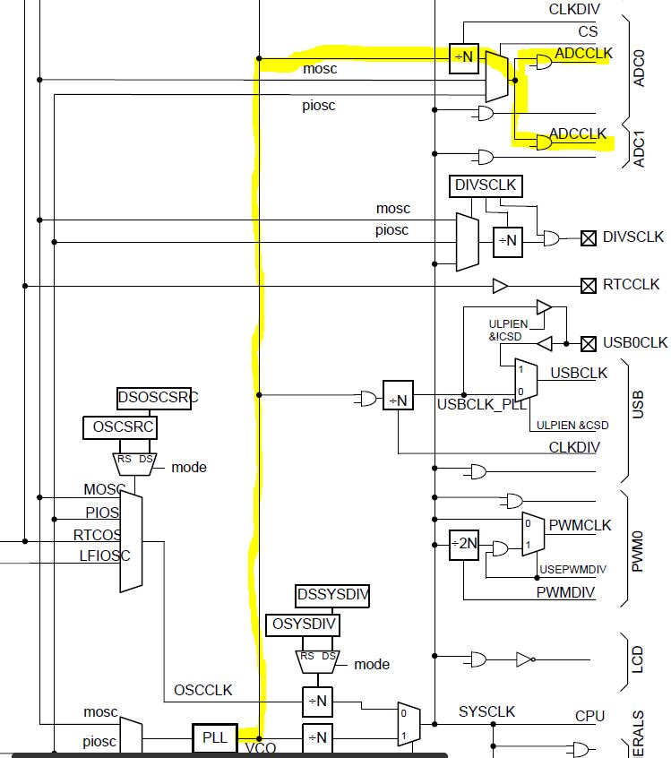
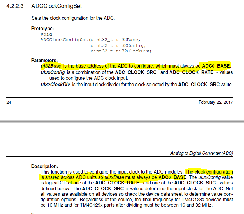
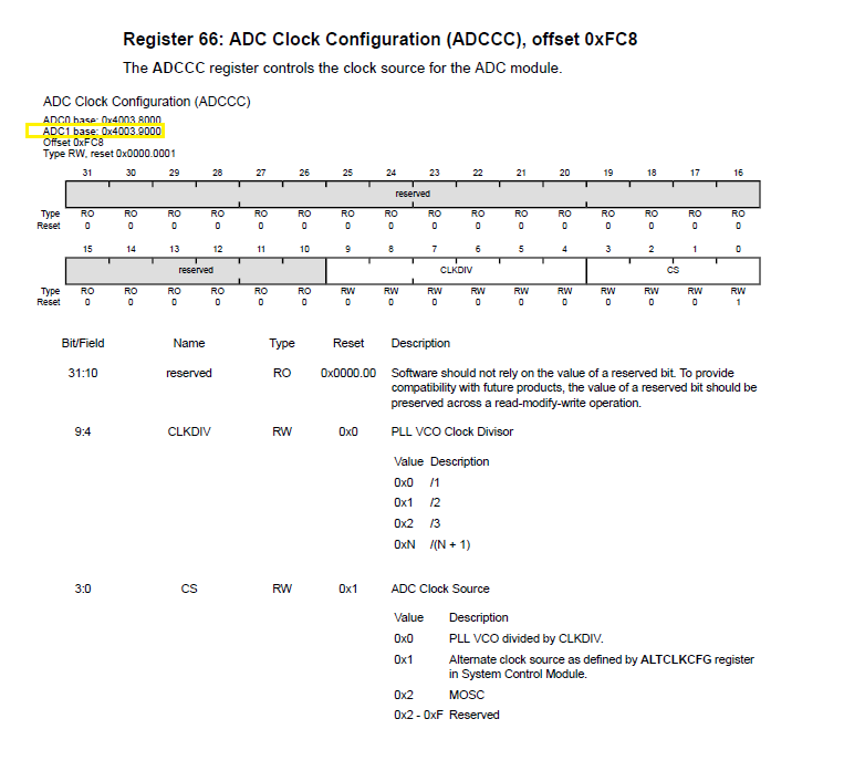
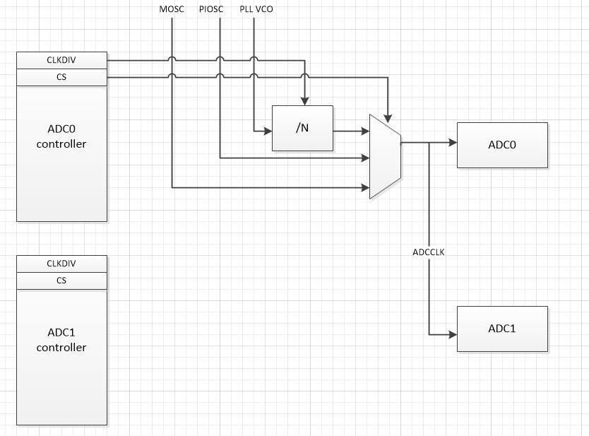
Strange issues of ADC1 temperature sensor reads and other unexplained sequencers behavior may be clock related. Past reading datasheet 15.3.2.7 states ADC0 sets the clock for the ADC module via ADCCC REG66. Most people would never think to check REG 66 that counters that statement when configuring the ADC clock via ADCClockConfigSet(). The ADC module contains both ADC0 and ADC1 blocks or peripherals. Seemingly the default ADC1 clock divisor 1 produces ADCCLK at PLL speed if it is not being configured, that is if REG 66 base address 0x4003.9000 is actually valid.
Register 66 showing ADC1 base address makes 15.3.2.7 statement odd when ADCClockConfigSet() is only called to configure ADCCC REG66 for 0x4003.8000 ADC module. It would seem a Typo exists to say ADC0 sets the modules clock most anyone believes refers to both ADC blocks. Recently discovered ADC1 base address too exists REG66 and ADCClockConfigSet() was called only once with ADC0 base address.
15.3.2.7 Module Clocking:The system clock must be at the same frequency or higher than the ADC clock. All ADC modules share the same clock source to facilitate the synchronization of data samples between conversion units, the selection and programming of which is provided by ADC0's ADCCC register. The ADC modules do not run at different conversion rates.
Do ADC0 and ADC1 blocks share the ADC modules same clock source or are the actually independent configured clock sources as being indicated in REG-66? Perhaps another good reason to illustrate the clock sources in the figures of peripheral blocks!
Hi Bob,
Yet register 66 directly contradicts figures and text written shared ADC block clock, Note "Not all values are available on all devices" statement. Recently discovered ADC1 ADCPP REG bit field (9:4 CH) RO indicates 24 channels being available. That again is another alarming artifact that ADC1 is not being configured correctly, since it is not a documented errata.
Don't like the fact register 66 base address contradicts the main clock tree figure and proceeding text. I don't want to believe the text source as peripheral base address offsets have control over the silicon. Seemingly datasheet analysis text was written without any regard of a base address being indicated for ADC1 clock source. Perhaps a supposition was formed by the technical writer by directly using the main clock tree for information relative to ADC1?
Why would anyone ever believe the register offset address was not correct or even required?
Yet what makes the text correct and the REG 66 ADC1 base address incorrect? Would it not seem incorrect to have ADCCC base address RW (0x4003.9000) if the clock is indeed shared?
Perhaps someone forgot to add the code configuring ADC1 ADCCC RW bits CLKDIV 9:4, CS 3:0 at the same time as ADC0 in ADCClockConfigSet()? Point being the call passes/requires an ADC module base address with no ASSERT to reject ADC1 base address.
Hi Charles,
Yet if we check ADC1; ADCCC, CLKDIV bit is 0x1, only if SW does not first configure ADC1 clock source. That alone seems to contradict any and all previous belief for ADC0/1 sharing the same clock source. Check it yourself and earlier attempts to use PWM0 GEN's triggers on ADC1 sequencers would cause rapid ADC1 results behavior. If we allow ADC0 clock source to run 480Mhz (CLKDIV=1) we get rapid samples as when ADC1 clock source is not configured (CLKDIV=1) versus ADC1 CLKDIV=15. Would normally agree with both at this point yet ADC1 was randomly returning very high value samples MCU AGND pin was connected to PCB AGND plane versus DGND trace run yet ADC0 samples triggered from PWM0 GEN1 was without issue.
Test issue yourself:
ui32Config0 = ADCClockConfigGet(ADC0_BASE, &ui32ClockDiv0); ui32Config1 = ADCClockConfigGet(ADC1_BASE, &ui32ClockDiv1); UARTprintf("> ADC0-VCO/DIV-->>:%i\r\n", ui32ClockDiv0); UARTprintf("> ADC1-VCO/DIV-->>:%i\r\n", ui32ClockDiv1);
I'm redrawing what is already shown in the Clock tree diagram in the datasheet. It is what it is. The CLKDIV and CS fields in the ADCCC register from the ADC0 is used to configure the ADCCLK to both the ADC0 ad ADC1. The CLKDIV and CS in the ADC1 controller even though there has no bearing on the ADCCLK to the ADC1 converter. It is up to you if you don't want to believe it.