This thread has been locked.

If you have a related question, please click the "Ask a related question" button in the top right corner. The newly created question will be automatically linked to this question.

CC430F5135: spurious emissions near the carrier frequency

Expert 6370 points
Part Number: CC430F5135
Other Parts Discussed in Thread: CC1190

Team,

we did RF measurements on one of our product based on CC430F and we noticed unexpected spurious emissions near the carrier frequency.

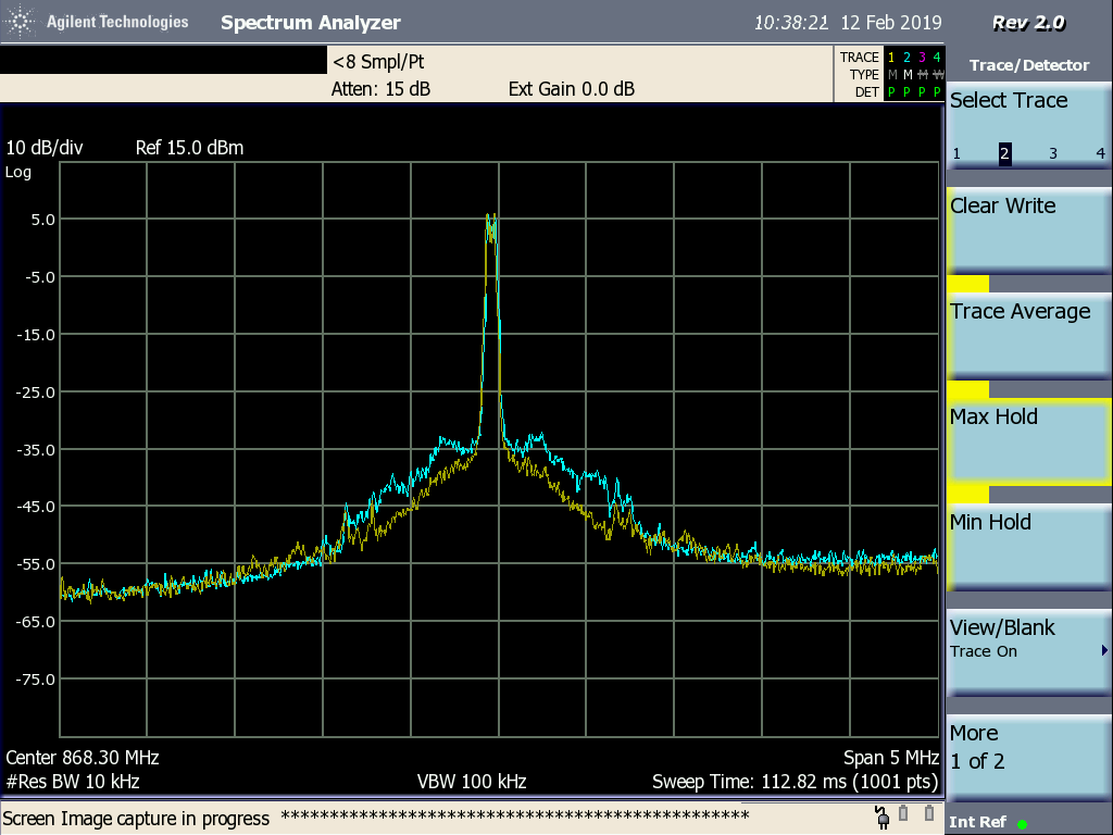
We did some experiments to investigate what is causing the unwanted emissions and we are not able to find the exact answer. We have the same PCBs with the same SW programmed but some of them have "good" spurious and some of them have spurious too high - see attached print screen of the measurement of spurious emissions near the carrier frequency.
The yellow trace is "good" and the blue is "bad".
We can share schematics and PCB layout offline if helpful.

Do you have any advise what part of HW could cause above mentioned spurious increase (perhaps xtal)?

The crystal frequency is 27,0 MHz. We would like to operate at 2 frequencies: 869,52 MHz and 868,3 MHz.

Thanks for your help
TI Customer

  • Does this mean that you always get the blue trace for a given PCB and always the yellow with a bad PCB? Does the spur follow the chip or PCB if you swap chip?

    These are close in spurs, which clause in ETSI 300 220 v3.1.1 are you failing?
  • Yes, you are correct: The PCB which has blue trace has always this result and the same for the "yellow" PCBs.

    We have not tried to swap the chip yet but we can try it.

    This is the 5.9 Unwanted emissions in the spurious domain - 5.9.1.1 Unwanted emissions for a TX mode.

    I forgot to mention that there is also the CC1190 RF Front End on the PCB - the schematic and the PCB layout corresponds to the reference design: CC1101–CC1190EM 869 MHz Reference Design (SWRR075.zip).

    Marek

  • Does that mean that the measurements are done after the CC1190? If that is the case, how does the signal look like on the output of the CC430 (To be more exact at the input of the SAW filter, with the SAW filter removed)? 

  • Yes, the measurements in the first post were done on the antenna connector (after the cc1190).

    We swapped the CC430 on "good" and "bad" PCBs and the "close spurious" followed the chip. So the differences are in the CC430...

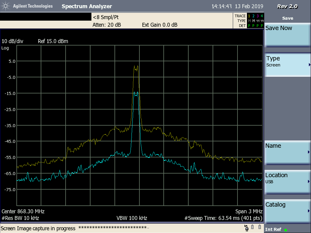
    We also measured the spurious at the input of SAW with SAW removed - You can see the result on the picture below. The yellow trace is the measurement on antenna connector (CC430+SAW+CC1190), the blue trace is at the input of SAW with SAW removed. I think that the result is the same (of course the power is lower without CC1190).

    Marek

  • - Are you going to use different output power settings in the two bands you want to operate in?
    - Could you show me the plot where you have measured against 5.9.1.1 and fail? The plots you have shows so far use the wrong detector and I assume that it's not an issue at fc+/-4*OCW and out which should be measured with 10 kHz.
  • - yes, we are going to use different output power settings in the two bands:

    1. fc = 868,25 MHz, CC430 reg. value = 0x23, ef. radiated power is approx. 12,0 dBm.

    2. fc = 869,52 MHz , CC430 reg. value = 0x3D, ef. radiated power is approx. 22,0 dBm.

    - I do not have the plots of measurement according 5.9.1.1 in certified laboratory. You are right that you can not see the "fail" conditions on my plots - my measurement is only informative, in conductive mode and are done on the antenna connector. The certification measurement was done in radiated mode with connected antenna with gain approx. +7dBi. The fail conditions happened around the 867,75 MHz with RBW 10 kHz, which is in the frequency range f c - m ≤ f < fc - n, as you stated.

    - I did my measurement only to investigate what causes the difference between the same PCBs with the same SW and register settings programmed.

  • The -36 dBm/ 10 kHz limit starts at fc - 4xOCW. How do you get 867.75 Mhz to be within this band? We get this to start at 868.3 MHz - 4*0.6MHz = 865.9 MHz.
  • If you use the band width, 600 kHz, as the OCW you are right. Our "certificate authority" used the bandwidth we declared and this was only 100 kHz (we do not use the whole band). I agree with you, we could get the PASS result of this certification test if we use the 600 kHz band width.

    But my question was what could cause the close spurious difference in the same PCBs, to make some improvements in the BOM, PCB layout, reg. settings etc. And now I know it - CC430 and we can do nothing.

    I think that we can close this thread.
  • The reason for my questions about how you measure, plots etc is that I have seen a lot of cases where the customer/ certification lab don't measure correctly.

    Since the issue seems to follow the chip I'm not sure how much can be done on the PCB but if you like I can take a quick look at it to see if I can see something that could explain this. Send me a friend request if you don't want to have the design open on the forum and send schematic as pdf and layout as gerber.