This thread has been locked.

If you have a related question, please click the "Ask a related question" button in the top right corner. The newly created question will be automatically linked to this question.

TM4C1294KCPDT: CADC discharge

Guru 54118 points
Part Number: TM4C1294KCPDT
Other Parts Discussed in Thread: LM3S8971, EK-TM4C1294XL, TIDA-00909

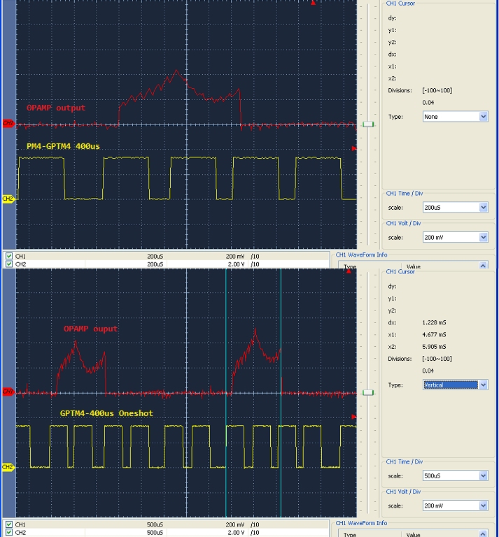
It is taking unreasonable 400us for ADC converter cycles of 3 specific AINx channels, required for CADC to discharge between samples. CADC charge voltage is reluctant to go below some arbitrary threshold yet the ANIx input level reduces well below 1/4 VREFP amplitude <80mV. Hence 400us between triggering conversions allow for CADC to reluctantly discharge back to the arbitrary threshold first established, though not correct. The OPAMP output is consider settled in 9.6us to 0.5% of final value so the ADC is messing up in these conversions.

The OPAMP's are coupled 4.87k series resistance into single ended AINx inputs. The OPAMPs present <1nf load to each AINx input. Seemingly OPAMP should easily discharge CADC during push/pull cycles yet does not. What is going wrong CADC remains charged to arbitrary threshold yet FIFO's return 0V results after sampling stops? Conversion Interrupt occurs for the 3 AINx only during 400us triggering via GPTM one shot intervals. Seemingly plenty of time exists for CADC to discharge following AINx voltage changes as they fall below 1/4 VREFP. The application even forces the sample variable to 0x0 after each MIN/MAX evaluation each interrupt cycle. The variables and FIFO values are being drained, tested for under/over flow conditions. The application handling of FIFO results is not the problem as the hardware is misbehaving around CADC for what ever reason. 

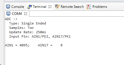
Why does CADC require so much time to discharge and what can be done in ADC configuration to correct behavior? The NSH set 0x4 or any other value has no effect to reduce the arbitrary CADC threshold, obviously floating FIFO value higher than AINx input voltage in this case.

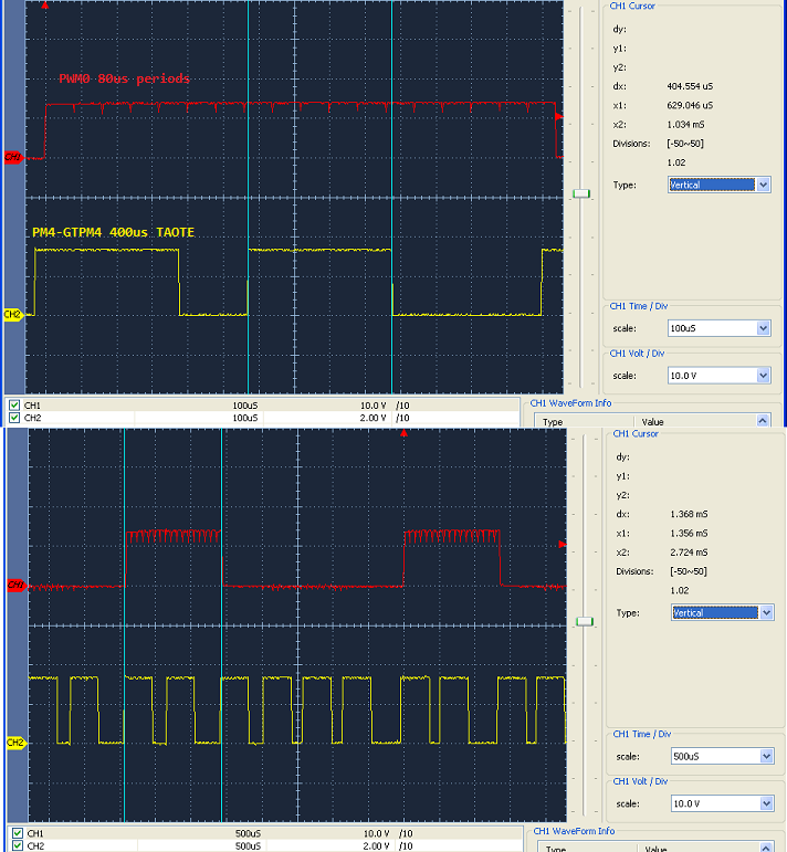
Scope captures indicate CADC being charged only >400us settling:

  • Are you comparing the expected ADC results to your original voltage or to the voltage on the 1nF capacitor?. The time constant of your 4.87K and 1nF is 5uS. The time constant for the ADC pin itself is 25nS (2.5K Ohm into 10pF). With ADC clock at 32Mhz and 4 cycle sample time, should get you to within 1%.
  • Hi Bob,

    I meant to say 1/4 VREFP above post and will edit. The OPAMP output represents <1nf load without sustained ringing, no other external capacitance to keep CADC charged.

    More investigation reveals samples below 1/4 VREFP or 4096/326 (18.123mV) are extremely noisy, even after 4/3 low pass filtering.
    Expecting 4mV/100mA precision from 40mV/1A input to 3 AINx. Oddly requires just under 6x80us PWM periods (480us) to get results in last PWM period <> 1/4 VREFP, 100mA up to 1A and 1A up to >20A. Same basic software used on Stellaris 10bit ADC, conversions <40us PWM periods with no added capacitors on AINx inputs or OPAMPS output.

    Not even after software update and 12bit precision ADC can it produce similar results below 1/4 VREFP via 4/3 LPF. Very odd TM4C1294 ADC requires 10x more settling time than LM3S8971. Some where 40us typical conversion settling has become 400us for the very same PWM frequency as Stellaris LM3S sampled via 50Mhz SYSCLK. There are six 80us PWM periods in each frame and only the last 80us period (@400us) can be sampled with any precision. That makes it seem as if CADC is not discharging during the other 5 PWM periods. That was my first thought as to why precision <18mV 1/4 VREP is nearly impossible to achieve via WA.

    How can the Stellaris 10bit SAR require less settling time (40us) than 12 bit SAR requiring (400us)? Perhaps something is not correct clocking ADC0 32Mhz and PWM module SYSCLK/2 or 60Mhz?????? Seemingly ADC0 is not in phase with PWM0 clock source by a factor of 10x. What else other than CADC explains why we can only sample the last PWM period @400us and no others with any precision???? What in clocking can cause 10x phase shift of ADC0 triggers from PWM modules clock source and make it seem CADC is not discharging?

  • I did a simple application on the EK-TM4C1294XL Launchpad that converts two channels. The ADC runs off of PIOSC at 16MHz, it uses the standard 4 cycle sample time and no hardware averaging. The first channel is at 3.3V and the second channel is at ground. The sample time is 250nS, and the sample capacitor discharged from 3.3V to less than 1mV in that time as shown by the printed output results. The issue you are seeing is not an inherent chip problem.

    /cfs-file/__key/communityserver-discussions-components-files/908/2768.ADCtwoChannel.zip

  • Hi Bob,

    The point is the addition of an OPAMP 1nf load into AINx coupled with 80us periodic pulses keep CADC >40mv after it has been initially charged. The odd part is the initial charge slope CADC (0-40mV) is extremely precise but the discharge slope (40-0mV) never occurs after the hold step reaches >40mV. That occurs when PWM0 is active on AHB and all other AINx remain fairly precise producing linear MCU temperature, DC-Volts, PCB temperatures etc. Only assumes PWM0 is indeed synchronous with/to ADC0 clock source as they both relate to AHB arbitration timing.

    Seemingly LM3S8971 400Mhz PLL kept 50Mhz SYSCLK/AHB timing between PWM0 and ADC0 exactly synchronous. Nobody would know if TM4C PLL was skewed until they confirm a closed loop can be maintained between both peripherals.

    The only time producing correct sample values <2.5us settling is during initial ramp (0-40mV) of PWM0 input signal into AINx. Otherwise each 80us sample goes rogue for 5 PMW cycles (400us). If triggering sequencer via PWM0, samples never settle to/with the actual analog voltage present on any one of 3 AINx. Timing is critical to produce the correct values based on interrupt handling in the closed loop between PWM0 and ADC0. If PWM0 is not exactly synchronous with ADC clock or AHB arbitration it might explain 400us settling would it not?

  • Interesting facts below LM3S8971 datasheet ADC0 clocking configures automatic 1MSPS sample clock divider (16.667mHz), not 16mHz or 30Mhz. Hence Tivaware ADCClockConfigSet() creates even sample clocks for (1-2MSPS) that may not be synchronous to PWM0 generator module (ADC0 Trigger Source) timing when SYSCLK being divided by 2.

    TM4C1294 SYSCLK 120mHz PWM0 clock @60mHz and ADC0-120mHz (1630mHz sequencer samples) appear to drift >400us apart after PWM0 becomes active. Seemingly CADC remains charged >40Mv never sampling PWM0 generated wave forms <40mV when ever it becomes active on AHB and CADC have charged >40mV. The sampling never aligns with valleys in PWM generated wave forms ADC0 attempts to monitor via GPTM or PWM trigger sources. Instead ADC0 samples >40mV from trigger source (GPTM) monitored analog signal present on AINx channels. PWM0 trigger source never samples >40mV once it reaches 40mV hence neither trigger source is producing correct reading <400us settling of CADC.

    12.2.2 Module Control: Outside of the sample sequencers, the remainder of the control logic is responsible for tasks such as:

    ■ Interrupt generation ■ Sequence prioritization ■ Trigger configuration

    Most of the ADC control logic runs at the ADC clock rate of 14-18 MHz. The internal ADC divider is configured automatically by hardware when the system XTAL is selected. The automatic clock divider configuration targets 16.667 MHz operation for all Stellaris® devices.

    Missing from TM4C1294 PWM0 module (PWMCC REG89) bitfield text present in LM3S8971 RCC REG8 bitfeild discription below:

    PWM Unit Clock Divisor (PWMDIV)

    This field specifies the binary divisor used to predivide the system clock down for use as the timing reference for the PWM module. This clocks only power 2 divide and rising edge is synchronous without phase shift from the system clock.


  • BP101,
    You switched topics on me. Can we agree that the issue is not the inherent time of the sample capacitor to stabilize to the new voltage? If so, I want to split this thread and put your questions about synchronizing the ADC to the PWM output in a separate thread.
  • HI Bob,

    This issue is beyond my expertise and only able to scratch the surface of what might be happening. What makes it necessary to configure GPTM4 >400us to sample along OPAMP output peaks >40mV AINx inputs? That seemed to work quite well with LM3S8971 @1MSPS but not via the TM4C1294 SAR ADC @1 or 2MSPS. How could TM4C1294 clocking be so different from LM3S8971 to affect CADC charge sharing?

    We should be able to trigger from the center of PWM 80us periods and produce very accurate sample results. Triggering of sequencer samples does not produce correct FIFO values even via GPTM Oneshot set <400us intervals. It seems something is effecting CADC charge sharing with basic OPAMP open loop gain occurring in the ADC configuration.

  • Hi Bob,

    My opinion obviously differs this thread ends in quantifying differences, Stellaris 10bit ADC to that of TM4C1294 12bit ADC. Seemingly difference in ADC designs limits CADC charge sharing via PWM0 triggering source of sequencers, perhaps from added NSH encoding. Back tracking is the only way to get at the nitty gritty to question, what is affecting CADC to charge 40us center of PWM pulses.

    Other engineers in the industry use M4F ADC with the exact sampling schema, PWM0 trigging sequencer center of PWM to sample OPAMP signals and do not report this same issue. Question moves for new post seeking to identify signals sampled via TAOTE control of sequencer versus PWM0 timing seem a possible WA. Alternatively what can be done to ADC configuration to disable NSH hold times as to determine why or what may lead to CADC refusing discharge <40mV or >40mV when PWM0 triggers sequencers synchronously to the center of duty cycle periods. Perhaps it dangerous for TI to maintain revision of ADC silicon if there is an issue being uncovered by great detective work, right?
  • Hi BP101,
    Yes our opinions do differ. You are convinced that there is a problem in the TM4C1294 device because with your hardware and your software you are not getting the results you expect. I have tried to open your mind to other possibilities by providing you an example project that can be easily run on a Launchpad that demonstrates the ADC can completely charge or discharge in a 250nS sample time. I cannot debug your code or your hardware for you. The device validation we did before releasing this part, my own testing and the fact that you are the only customer out of thousands who claims there is an issue with the ADC sample timing of the TM4C1294 support my current opinion. You made a claim our part does not work properly. I investigated the claim, found it not to be true and then provided you a test case which disproves your claim. There is no point in discussing further the inherent ability of the TM4C1294 to charge the sample capacitor.

    Don't get me wrong. I understand you have a system problem. I suggest you evaluate:
    1. the source impedance
    2.the actual voltage at the pin
    3. the actual timing of the ADC sample. (using an interrupt to fire a general purpose timer leaves you subject to interrupt latency if any other interrupts are being used in your system.)

    If part of your system is not working, simplify it. Create a new project that just does that function. You will have more success putting together small working parts than trying to debug an entire system at once.
  • Hi Bob,

    You really do need to add some PWM triggering to your project as it misses point CADC is not function correctly for general use with center PWM triggering of sequencers. I suspect CADC charging never has been  evaluated when properly draining of FIFO after reading samples during interrupt events. Again LM3S8971 not being effected since it does not have NSH encoding constraints during FIFO draining. Seemingly reverse current is flowing from the FIFO register into CADC keeping it charged to specific RC time constant of the PWM 80us periods.  That being a relatively slow period CADC is being greatly effected by RC time constant of FIFO events handling.

    A proper code example must drain FIFO during each interrupt event and after reading or the results data can be under/over flow without notice until perhaps test code eventually faults a sequencer. It is apparent Tivaware is not following proper FIFO reading or handling of flag events and leads several engineers to make false assumptions of hardware being without issues. Seemingly NSH hold values may also cause FIFO values being lower during CADC charge events when FIFO results are cleared after Reading (POP) register values. It would seem the major difference between MCU family is the addition of NSH being the culprit of TM4C1294 inoperability. If the FIFO is not drained after reading samples into C+ array the TPTR/HPTR register become inactive, besides the RC time constant of CADC being badly effected in the process.

    Bob Crosby said:
    If part of your system is not working, simplify it. Create a new project that just does that function. You will have more success putting together small working parts than trying to debug an entire system at once.

    The simplified WA uncovers CADC timing issue via oneshot timer (TAOTE) triggers sequencer 40x slower versus center PWM events. This trigger method allows 400us between sample acquisitions giving CADC huge window for charge/discharge time correcting improper ADC behavior around FIFO results clearing. The datasheet is not disclosing how FIFO reading (POP) also effects CADC time constants/charge level and I suspect no one is even aware of this odd errata. My opinion is reading the FIFO should not effect CADC in any way yet it does in a very bad way with PWM0 high speed triggering. 

    Bob Crosby said:
    3. the actual timing of the ADC sample. (using an interrupt to fire a general purpose timer leaves you subject to interrupt latency if any other interrupts are being used in your system.)

    So why does TAOTE timer method work far better than triggering center of PWM periods which effects FIFO results data based on CADC acquisition steps?

    Don't get me wrong I only seek to identify this failure so TI produces a corrected future ADC module where rapidly reading FIFO results data can not directly impact CADC charge events as it now does. It seems the CADC acquisition steps are in odd hold state based on RC time constant derived from FIFO read results time frames of PWM0 high speed triggering.

  • BP101 said:
    Seemingly reverse current is flowing from the FIFO register into CADC keeping it charged to specific RC time constant of the PWM 80us periods.

    No, that is not possible. The ADC is an analog macro done in 3V logic, the FIFO is all digital in the 1.2V domain. Your conclusion does not make sense from a chip design point of view.

    Again, I suggest you not look inside the chip for the problem. If there were such a fundamental problem in the device, others would see it too. Verify your voltage at the pin and that you are sampling at the correct time. Check for FIFO overflow in your interrupt routine.

  • Hi Bob,

    Bob Crosby said:
    No, that is not possible. The ADC is an analog macro done in 3V logic, the FIFO is all digital in the 1.2V domain. Your conclusion does not make sense from a chip design point of view

    Ok yet CADC is simply not charge sharing center of 80us periods. The CADC values sampled remain very low FIFO read results. Yet if the trigger conversion is given 400µs between samples, CADC seems to share charge and acquisition the signal >40mV but never discharges again <40mV. So the signal can marginally be sampled but not at PWM0 trigger speeds. When we try to sample signal 20x gain CADC refuses to charge share <400us settling for signals >50-80mV, some where in that range. Long as the analog signal amplitude never exceeds say 80mV, CADC charge sharing cycles occur at PWM0 trigger speeds via the same SW. 

    Same OPAMP works correctly via Piccolo ADC TIDA-00909, perhaps something is not being disclosed in TM4C datasheet we need to know to make it work the same? Should customers have to reduce or alter amplifier gain in order for the TM4C ADC to properly charge share at PWM0 trigger speeds?   

    Bob Crosby said:
    Again, I suggest you not look inside the chip for the problem. If there were such a fundamental problem in the device, others would see it too.

    Seemingly an assumption on your behalf that others are using the same TI amplifiers with TM4C1294 and never having this issue.   

    The samples align with reading of the FIFO results, verified via GPTM output pin. Yet the FIFO values never settle <400us or fall below 40mV once CADC has been charged to or beyond that valance level once the 20x gain signal becomes >80mV or so.

  • Below scope capture indicates samples via 400us Oneshot GPTM, versus PWM0 high speed triggering. Two samples @400us is all ADC can resolve via CADC charge share for the OPAMP signal reposted top of thread. PWM0 CH1 takes roughly 8 80us periods for CADC settle to 1/2 LSB. Should we be able to trigger sequencer via PWM0 to sample 20x gain analog signal? Seemingly there is an limitation TM4C can not sample (periodic) signals at PWM0 40us trigger speeds above a certain gain and properly acquisition the signal to 1/2 LSB. Such a restriction to amplifier gain allows error % to increase beyond mathematical predictability of SW to correctly determine any hardware changes made to reduce said gain. There in lies the paradox as to why PWM0 high speed triggering of sequencer samples breaks down in two distinct ways. 

    What is so different between Piccolo ADC TIDA-00909 as it properly acquisitions 10-25us periodic signal with same 20x amplifier gain? Might the sinusoidal attribute be an explanation for how CADC charge share behaves in 20x gain?

  • Hi Bob,

    Interesting the Nyquist rate or sample conversion rate in this case 400us(2500Hz) is 10x slower than 1/2 the PWM frequency (12.5KHz) or 25KHz, Nyquist rate. The OPAMP bandwidth is 400KHz and ADC sample rate 2MSPS via 32Mhz ADC clock.

    Seemingly the PWM clock is not synchronous with ADC clock by a factor of 10x and triggering precision conversions fail @40us(25KHz). Thus PWM center triggered conversion causes aliasing at twice the Nyquist rate sample component, (25KHz). Samples are seemingly off by several hundred electrical degrees in the high speed conversions. The question is why is the Nyquist sample rate needing to be slowed well below 25KHz in order to achieve precision signal acquisition?

    I am unaware of how PWM clock rate (60MHz) relates to the ADC conversion clock rate (32MHz) in the Nyquist sample rate. Why is the correct Nyquist rate not possible to accurately acquisition signal CH1 created by PWM0 and converted by ADC0 clock sources? Obviously if your test example proves the ADC can sample 1mV then something else is not correct that cases CADC to remain charged >40mV and <80mV in 25KHz conversions of PWM triggers. We need basic peripheral clocking diagrams to be able to figure this issue out. TI has not provided necessary information in datasheet to accomplish this task in the field. Configuring ADC0, PWM0 60MHz did not make a difference and ADC0 clock 16Mhz (1MSPS) only slight difference in sample magnitude was noticed.

    The Talk tab top paragraph adds another engineers view on the Wikipedia topic.

    https://en.wikipedia.org/wiki/Nyquist_frequency&nbsp;