


Other Parts Discussed in Thread: REF3130, TMS320F28379D, CONTROLSUITE, C2000WARE
Dear All,
We are working on TMS320F28377S. We are using DAC - B to set output current limit of external module.
We are using TI's REF3130 reference voltage source. We observed the reference voltage as 2.0085V
As per datasheet the DAC output expected within +/-5 LSB range.
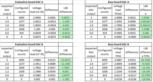
While testing we observed the DAC output has variation 9 to 16 LSB (Refer base board DAC B)
To analyze the observation, we validate the result with other DAC channel and with TMS320F28379D evaluation board.
As shown below with DAC A on our developed board, we found the variation within expected 5 LSB (Refer base board DAC A)
With TMS320F28379D evaluation board,
- For DAC A variation observed 0 to 8 LSB
- For DAC B variation observed 1 to 12 LSB
We used sample code for testing from bellow link for testing.
C:\ti\controlSUITE\device_support\F2807x\v210\F2807x_examples_Cpu1\buffdac_enable\cpu01\ccs
Just changed REFERENCE and ADC channel as below . Attached is the code used for testing.
#define REFERENCE REFERENCE_VREF
#define DAC_NUM DACA
Our queries:
On our board, we observed good result for DAC A (within expected +/- 5 LSB variation) against DAC B. On evaluation board, we observed good result for DAC A against DAC B.
On our board, for 0 count input to DAC B, we observed offset of 0.0136V.
1) What might be the possible reason for DAC A gives good result against DAC B?
2) On our board, how we can get DAC B output within expected +/- 5 LSB variation?
3) On our board for DAC B, how we can can overcome offset of 0.0136V for 0 count setting? What is the reason for this high offset ?
Regards...
Yogesh


