This thread has been locked.

If you have a related question, please click the "Ask a related question" button in the top right corner. The newly created question will be automatically linked to this question.

TMS320F280039C: what is the tolerated voltage ripple for VDDIO? Large voltage ripple will cause the TMDSEMU110-U Debug probe failed connecting?

Part Number: TMS320F280039C
Other Parts Discussed in Thread: TMDSEMU110-U

Hi experts, 

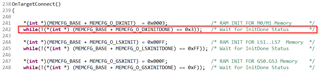
In customer's field, the TMDSEMU110-U debug probe can't connect to the target and prompts that the device is in low-power mode. 

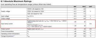
We find that when 3.3V VDDIO has larger voltage ripple (ripple = ±0.2V, due to connecting to IGBT driver board), the above phenomenon will happen. But when not connecting the driver board, the 3.3V VDDIO is smoother, and the debugger can work as expected. 

So I want to know the root cause of this failed target-connection, due to MCU itself or XDS110 debugger or both? What is the tolerated voltage ripple for DSP and XDS110 debugger to work fine? 

Best Regards, 

Will 

  • Additional information: they uses internal VREG LDO to generate 1.2V VDD (ripple=±0.1V when connecting to driver board) and the debugger can't read register ST1. GEL will stop at the following while loop: 

    Furthermore, sometimes they can connect to target but after few seconds it will get into No power-clock again. 

  • Hi Will,

    Looks like when you connect IGBT driver board there is high current condition happening (maybe a short) which might be causing the VDDIO voltage to droop. 0.2V ripple should be tolerated but it may be also clamping on the instantaneous current requirements. What is the current rating on the external regulator used to supply VDDIO?

    Also, can you capture VDDIO supply when you connect IGBT driver board? Also a possibility that VDDIO voltage might go below Vmin/BOR voltage causing the device to reset/disconnect.

    Best Regards,

    Nirav

  • Hi Nirav, 

    Thanks for your reply.

    Also, can you capture VDDIO supply when you connect IGBT driver board? Also a possibility that VDDIO voltage might go below Vmin/BOR voltage causing the device to reset/disconnect.

    The customer has captured the VDDIO supply and the XRS pin, the device is not BOR reset and the VDDIO voltage is range from 3.422V to 3.216V when connect the IGBT driver board. 

    What is the current rating on the external regulator used to supply VDDIO?

    It is hard to measure this current. What is the effect of clamping on the instantaneous current requirements? Do you mean the following maximum ratings? 

    Will it influent the signal integrity of JTAG pin? I have let customer to measure the JTAG pins' waveform. 

    Thanks, 

    Will 

  • Hi Will,

    Good to know that VDDIO supply is ok and there is no BOR trip. Did the customer monitor XRSn pin also to see if that is not tripping?

    I was asking for a current clamp for the VDDIO supply and not input current. The table snippet is for the input current clamp.

    If there is a short circuit due to the connection to IGBT drivers it may cause a latch-up event in turn disconnecting the JTAG connection. Yes, input current may impact JTAG signal integrity.

    Yes, it will be good to monitor JTAG signals.

    Best Regards,

    Nirav

  • Hi Nirav, 

    If there is a short circuit due to the connection to IGBT drivers it may cause a latch-up event in turn disconnecting the JTAG connection.

    Do you mean that the VDDIO current clamp will lead to disconnection of some other IO pins? I don't find any related statements in Datasheet. So please give more comments on this. 

    What are possible causes for VDDIO current clamp? 

    Best Regards, 

    Will 

  • Hi Will,

    We do not specify the current clamp in the datasheet, but the typically latch-up event may occur at ~100mA. Again, I am not sure if that is the failure mode here, if we can check the JTAG signals when the IGBT board is connected will help.

    Is customer using Internal Vreg or supplying VDD externally?

    Best Regards,

    Nirav

  • Hi Nirav, 

    They are using internal VREG. Will let customer to capture the JTAG waveforms. 

    BTW, they place a 22ohm resistance in path of JTAG signals. Is this needed for XDS110 debugger (the frequency is lower than 10 MHz) ?  

    Best Regards, 

    Will 

  • Hi Will,

    What is the distance from JTAG header to the MCU? Regardless it is always a good practice to provide termination resistor. Please refer to below user guide which talks about transmission line effect and requirements of termination resistor depending on emulator.

    https://www.ti.com/lit/ug/spru655i/spru655i.pdf

    Best Regards,

    Nirav

  • Hi Nirav, 

    Thanks for your sharing.

    The customer has further finding: when they improve the limit current of the external power supply of control board (12V power supply equipment), the debugger can connect to the target even IGBT driver board connected.

    In order to figure out why this method can work, I let them modify the GEL file and remove the GEL_reset() in OnTargetConnect and adjust the limit current to original one (Because I think maybe due to resetting the MCU will recycle the power on-off of IGBT driver board, so the power supply will have a high-power pulse and exceed the limit current. ). But not succeed. 

    It is strange and I don't know why. Anyway, I think it can be an debug choice for other engineers. 

    Best Regards, 

    Will