This thread has been locked.

If you have a related question, please click the "Ask a related question" button in the top right corner. The newly created question will be automatically linked to this question.

TMS320F280021-Q1: C2000 ADC Wrong Reading Values

Part Number: TMS320F280021-Q1

Hi, 

I am have an issue reading the raw values from the ADC for voltage measurement
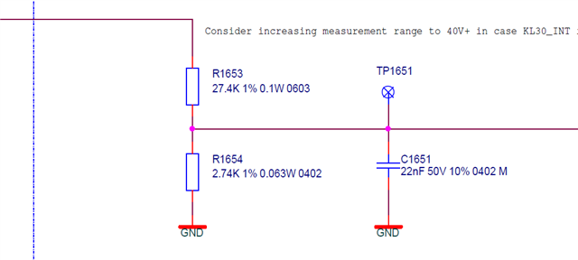
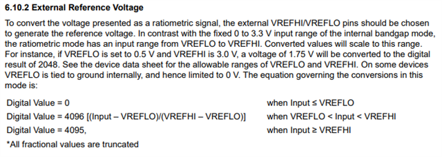
I have applied voltage 1.1V on the adc pin, and external VREFHI is 3.3V and VREFLO is grounded

So according to this formula I should I get a raw value of 1365. Although the ADC reading value is 1410 

Any recommendation what could be the reason behind this?

Thank you

  • Hi Mohamed,

    The result of ADC conversion depends mainly on the accuracy of reference signal and the input signal being converted.  The conversion result you are getting is off by 45 codes.  How accurate are the 3.3V reference and the 1.1V input signals that were used and what is the resolution of the voltmeter used to measure these levels?  Results of conversion is also influenced by the impedance of the analog input channel used.  Any resistance and capacitance on the pin would affect sample and hold time settings that would be sufficient to charge the internal sampling capacitor of the ADC.  More on this topic is available on the Technical Reference Manual section 15.13.2 (Choosing and Acquisition Window Duration).

    Regards,

    Joseph

  • Hi Joseph,

    The measurements for the reference and input are accurate (3.3V and 1,099V) 
    the voltmeter accuracy is +/- 1%
    There's a voltage divider connected to the ADC pin for which I considered the Resistance and capacitor value when I calculated the Acquisition window which is in my case 35ns 
    There's a deviation in all ADC pins measurements up to 78 codes
    I have no clue what might be the issue for this deviation of all mentioned is considered

    I am looking forward for your reply

  • Hi Mohamed,

    Let's take a look at the voltage divider and capacitor in your input circuit.  Can you share the values?  Can you also share the ACQPS settings, system clock (SYSCLK) speed and the ADC prescaler setting?  Just wanted to have a quick check that sampling time is sufficient considering the resistor divider input network and capacitance.

    Regards,

    Joseph

  • Hi Joseph,

    Please find screenshot attached for the voltage divider 

    Can you also share the ACQPS settings: 10ns


    system clock (SYSCLK): 100MHz
    the ADC prescaler setting: input CLK/2 

    Thank you

  • Hi Mohamed,

    Based from the values of resistances and capacitances in the input circuit, you are not allowing enough time for the sampling capacitor in the ADC to charge.  What I have come up with is that the effective RS (27.4K||2.74K = ~2.41K) and 22nF input capacitor will produce a time constant of (T) of  ~53uS based from Section 15.13.2 (Choosing An Acquisition Window) in the TRM. The number of time constants (k) came out to be ~1.3.  Total sampling time needed would be T*k and it came out to be ~69.7uS so ACQPS value would be 6971, however the ACQPS register only has a maximum value of 511 so the signal is not being allowed enough time to charge the internal ADC sampling capacitor.

    Bottomline is that you need to minimize the input impedances to satisfy the time constants and settling error as described in section 15.13.2 in the TRM,  Since you are probably reducing the input signal from the large input voltage, you would need to have those higher value of resistances for the voltage divider to produce the correct level for the ADC input, but this also causes settling issues as described above.  To remedy this, you can introduce a unity gain buffer at the output of the voltage divider to increase the signal drive and isolate the high impedance side from the ADC input.

     Here are a also a couple of helpful app notes that discusses signal conditioning in addition to the notes on the TRM that will be applicable for the scenario that you are having:

    Regards,

    Joseph