Dear TI Support Team,
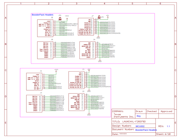
I am currently working on a project that involves connecting a thermistor to the ADC pins of a development board using the TMS320 C2000 MCU. I've located pins A0, A1, D0, and D1 on the schematic, which are associated with the J9 connector (as seen in the attached image), but I am unable to find this connector or the corresponding pins on the physical board itself.
//#############################################################################
//
// FILE:   adc_ex1_soc_software.c
//
// TITLE:  ADC Software Triggering
//
//! \addtogroup driver_example_list
//! <h1>ADC Software Triggering</h1>
//!
//! This example converts some voltages on ADCA and ADCD based on a software
//! trigger.
//!
//! The ADCD will not convert until ADCA is complete, so the ADCs will not run
//! asynchronously. However, this is much less efficient than allowing the ADCs
//! to convert synchronously in parallel (for example, by using an ePWM
//! trigger).
//!
//! \b External \b Connections \n
//!  - A0, A1, D2, and D3 should be connected to signals to convert
//!
//! \b Watch \b Variables \n
//! - \b adcAResult0 - Digital representation of the voltage on pin A0
//! - \b adcAResult1 - Digital representation of the voltage on pin A1
//! - \b adcDResult0 - Digital representation of the voltage on pin D2
//! - \b adcDResult1 - Digital representation of the voltage on pin D3
//!
//
//#############################################################################
//
// $Release Date: $
// $Copyright:
// Copyright (C) 2013-2023 Texas Instruments Incorporated - http://www.ti.com/
//
// Redistribution and use in source and binary forms, with or without
// modification, are permitted provided that the following conditions
// are met:
//
//   Redistributions of source code must retain the above copyright
//   notice, this list of conditions and the following disclaimer.
//
//   Redistributions in binary form must reproduce the above copyright
//   notice, this list of conditions and the following disclaimer in the
//   documentation and/or other materials provided with the
//   distribution.
//
//   Neither the name of Texas Instruments Incorporated nor the names of
//   its contributors may be used to endorse or promote products derived
//   from this software without specific prior written permission.
//
// THIS SOFTWARE IS PROVIDED BY THE COPYRIGHT HOLDERS AND CONTRIBUTORS
// "AS IS" AND ANY EXPRESS OR IMPLIED WARRANTIES, INCLUDING, BUT NOT
// LIMITED TO, THE IMPLIED WARRANTIES OF MERCHANTABILITY AND FITNESS FOR
// A PARTICULAR PURPOSE ARE DISCLAIMED. IN NO EVENT SHALL THE COPYRIGHT
// OWNER OR CONTRIBUTORS BE LIABLE FOR ANY DIRECT, INDIRECT, INCIDENTAL,
// SPECIAL, EXEMPLARY, OR CONSEQUENTIAL DAMAGES (INCLUDING, BUT NOT
// LIMITED TO, PROCUREMENT OF SUBSTITUTE GOODS OR SERVICES; LOSS OF USE,
// DATA, OR PROFITS; OR BUSINESS INTERRUPTION) HOWEVER CAUSED AND ON ANY
// THEORY OF LIABILITY, WHETHER IN CONTRACT, STRICT LIABILITY, OR TORT
// (INCLUDING NEGLIGENCE OR OTHERWISE) ARISING IN ANY WAY OUT OF THE USE
// OF THIS SOFTWARE, EVEN IF ADVISED OF THE POSSIBILITY OF SUCH DAMAGE.
// $
//#############################################################################
//

//
// Included Files
//
#include "driverlib.h"
#include "device.h"

//
// Defines
//
#define EX_ADC_RESOLUTION       12
// 12 for 12-bit conversion resolution, which supports (ADC_MODE_SINGLE_ENDED)
// Sample on single pin (VREFLO is the low reference)
// Or 16 for 16-bit conversion resolution, which supports (ADC_MODE_DIFFERENTIAL)
// Sample on pair of pins (difference between pins is converted, subject to
// common mode voltage requirements; see the device data manual)

//
// Globals
//
uint16_t adcAResult0;
uint16_t adcAResult1;
uint16_t adcDResult0;
uint16_t adcDResult1;

//
// Function Prototypes
//
void initADCs(void);
void initADCSOCs(void);

//
// Main
//
void main(void)
{
    //
    // Initialize device clock and peripherals
    //
    Device_init();

    //
    // Disable pin locks and enable internal pullups.
    //
    Device_initGPIO();

    //
    // Initialize PIE and clear PIE registers. Disables CPU interrupts.
    //
    Interrupt_initModule();

    //
    // Initialize the PIE vector table with pointers to the shell Interrupt
    // Service Routines (ISR).
    //
    Interrupt_initVectorTable();

    //
    // Set up ADCs, initializing the SOCs to be triggered by software
    //
    initADCs();
    initADCSOCs();

    //
    // Enable Global Interrupt (INTM) and realtime interrupt (DBGM)
    //
    EINT;
    ERTM;

    //
    // Loop indefinitely
    //
    while(1)
    {
        //
        // Convert, wait for completion, and store results
        //
        ADC_forceMultipleSOC(ADCA_BASE, (ADC_FORCE_SOC0 | ADC_FORCE_SOC1));

        //
        // Wait for ADCA to complete, then acknowledge flag
        //
        while(ADC_getInterruptStatus(ADCA_BASE, ADC_INT_NUMBER1) == false)
        {
        }
        ADC_clearInterruptStatus(ADCA_BASE, ADC_INT_NUMBER1);

        ADC_forceMultipleSOC(ADCD_BASE, (ADC_FORCE_SOC0 | ADC_FORCE_SOC1));
        //
        // Wait for ADCD to complete, then acknowledge flag
        //
        while(ADC_getInterruptStatus(ADCD_BASE, ADC_INT_NUMBER1) == false)
        {
        }
        ADC_clearInterruptStatus(ADCD_BASE, ADC_INT_NUMBER1);

        //
        // Store results
        //
        adcAResult0 = ADC_readResult(ADCARESULT_BASE, ADC_SOC_NUMBER0);
        adcAResult1 = ADC_readResult(ADCARESULT_BASE, ADC_SOC_NUMBER1);
        adcDResult0 = ADC_readResult(ADCDRESULT_BASE, ADC_SOC_NUMBER0);
        adcDResult1 = ADC_readResult(ADCDRESULT_BASE, ADC_SOC_NUMBER1);

        //
        // Software breakpoint. At this point, conversion results are stored in
        // adcAResult0, adcAResult1, adcDResult0, and adcDResult1.
        //
        // Hit run again to get updated conversions.
        //
        ESTOP0;
    }
}

//
// Function to configure and power up ADCs A and C.
//
void initADCs(void)
{


    //
    // Set ADCDLK divider to /4
    //
    ADC_setPrescaler(ADCA_BASE, ADC_CLK_DIV_4_0);
    ADC_setPrescaler(ADCD_BASE, ADC_CLK_DIV_4_0);

    //
    // Set resolution and signal mode (see #defines above) and load
    // corresponding trims.
    //
#if(EX_ADC_RESOLUTION == 12)
    ADC_setMode(ADCA_BASE, ADC_RESOLUTION_12BIT, ADC_MODE_SINGLE_ENDED);
    ADC_setMode(ADCD_BASE, ADC_RESOLUTION_12BIT, ADC_MODE_SINGLE_ENDED);
#elif(EX_ADC_RESOLUTION == 16)
    ADC_setMode(ADCA_BASE, ADC_RESOLUTION_16BIT, ADC_MODE_DIFFERENTIAL);
    ADC_setMode(ADCD_BASE, ADC_RESOLUTION_16BIT, ADC_MODE_DIFFERENTIAL);
#endif

    //
    // Set pulse positions to late
    //
    ADC_setInterruptPulseMode(ADCA_BASE, ADC_PULSE_END_OF_CONV);
    ADC_setInterruptPulseMode(ADCD_BASE, ADC_PULSE_END_OF_CONV);

    //
    // Power up the ADCs and then delay for 1 ms
    //
    ADC_enableConverter(ADCA_BASE);
    ADC_enableConverter(ADCD_BASE);

    DEVICE_DELAY_US(1000);
}

//
// Function to configure SOCs 0 and 1 of ADCs A and C.
//
void initADCSOCs(void)
{
    //
    // Configure SOCs of ADCA
    // - SOC0 will convert pin A0.
    // - SOC1 will convert pin A1.
    // - Both will be triggered by software only.
    // - For 12-bit resolution, a sampling window of 15 (75 ns at a 200MHz
    //   SYSCLK rate) will be used.  For 16-bit resolution, a sampling window
    //   of 64 (320 ns at a 200MHz SYSCLK rate) will be used.
    // - NOTE: A longer sampling window will be required if the ADC driving
    //   source is less than ideal (an ideal source would be a high bandwidth
    //   op-amp with a small series resistance). See TI application report
    //   SPRACT6 for guidance on ADC driver design.
    //

#if(EX_ADC_RESOLUTION == 12)
    ADC_setupSOC(ADCA_BASE, ADC_SOC_NUMBER0, ADC_TRIGGER_SW_ONLY,
                 ADC_CH_ADCIN0, 15);
    ADC_setupSOC(ADCA_BASE, ADC_SOC_NUMBER1, ADC_TRIGGER_SW_ONLY,
                 ADC_CH_ADCIN1, 15);
#elif(EX_ADC_RESOLUTION == 16)
    ADC_setupSOC(ADCA_BASE, ADC_SOC_NUMBER0, ADC_TRIGGER_SW_ONLY,
                 ADC_CH_ADCIN0, 64);
    ADC_setupSOC(ADCA_BASE, ADC_SOC_NUMBER1, ADC_TRIGGER_SW_ONLY,
                 ADC_CH_ADCIN1, 64);
#endif

    //
    // Set SOC1 to set the interrupt 1 flag. Enable the interrupt and make
    // sure its flag is cleared.
    //
    ADC_setInterruptSource(ADCA_BASE, ADC_INT_NUMBER1, ADC_SOC_NUMBER1);
    ADC_enableInterrupt(ADCA_BASE, ADC_INT_NUMBER1);
    ADC_clearInterruptStatus(ADCA_BASE, ADC_INT_NUMBER1);

    //
    // Configure SOCs of ADCD
    // - SOC0 will convert pin D2.
    // - SOC1 will convert pin D3.
    // - Both will be triggered by software only.
    // - For 12-bit resolution, a sampling window of 15 (75 ns at a 200MHz
    //   SYSCLK rate) will be used.  For 16-bit resolution, a sampling window
    //   of 64 (320 ns at a 200MHz SYSCLK rate) will be used.
    // - NOTE: A longer sampling window will be required if the ADC driving
    //   source is less than ideal (an ideal source would be a high bandwidth
    //   op-amp with a small series resistance). See TI application report
    //   SPRACT6 for guidance on ADC driver design.
    //

#if(EX_ADC_RESOLUTION == 12)
    ADC_setupSOC(ADCD_BASE, ADC_SOC_NUMBER0, ADC_TRIGGER_SW_ONLY,
                 ADC_CH_ADCIN2, 15);
    ADC_setupSOC(ADCD_BASE, ADC_SOC_NUMBER1, ADC_TRIGGER_SW_ONLY,
                 ADC_CH_ADCIN3, 15);
#elif(EX_ADC_RESOLUTION == 16)
    ADC_setupSOC(ADCD_BASE, ADC_SOC_NUMBER0, ADC_TRIGGER_SW_ONLY,
                 ADC_CH_ADCIN2, 64);
    ADC_setupSOC(ADCD_BASE, ADC_SOC_NUMBER1, ADC_TRIGGER_SW_ONLY,
                 ADC_CH_ADCIN3, 64);
#endif

    //
    // Set SOC1 to set the interrupt 1 flag. Enable the interrupt and make
    // sure its flag is cleared.
    //
    ADC_setInterruptSource(ADCD_BASE, ADC_INT_NUMBER1, ADC_SOC_NUMBER1);
    ADC_enableInterrupt(ADCD_BASE, ADC_INT_NUMBER1);
    ADC_clearInterruptStatus(ADCD_BASE, ADC_INT_NUMBER1);
}
Could you please assist me in identifying where the J9 connector is situated on the development board? Furthermore, I would appreciate guidance on how to access the A0, A1, D0, and D1 pins for ADC connection to my thermistor.
Thank you for your assistance.
Nero