This thread has been locked.

If you have a related question, please click the "Ask a related question" button in the top right corner. The newly created question will be automatically linked to this question.

TMS320F28386D-Q1: SDFM clock

Part Number: TMS320F28386D-Q1
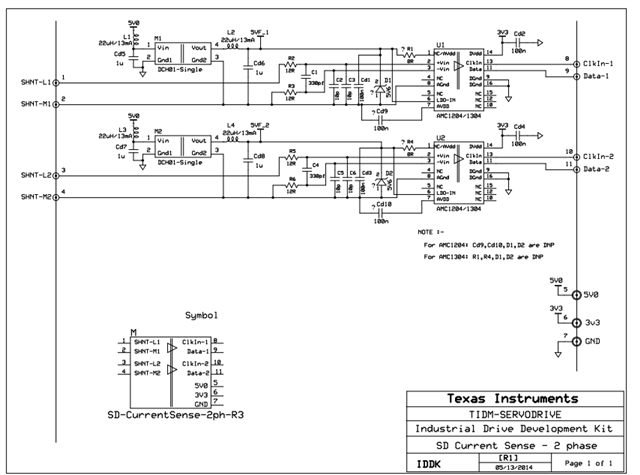
Other Parts Discussed in Thread: AMC1306M05, TIDM-SERVODRIVE, AMC1204, SYSCONFIG

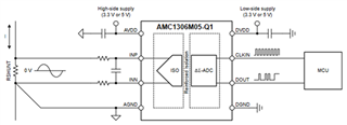
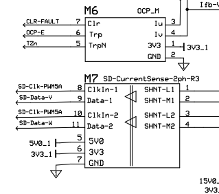
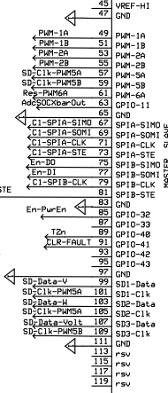
I'm working on a design with a TMS320F28386 DSP and an array of AMC1306M05 isolated sigma-delta ADCs sensing current.

I have a basic hook up question and I can't seem to find a good answer in the documentation.

Why does the F28386 datasheet refer to the SDFM clocks as inputs? They're referred to as inputs in the pin attributes table, Figure 7-36 SDFM block diagram, and in the digital signals table (Table 6-3).

I'm confused as these are obviously clock outputs that supply the modulation clock to the external sigma-delta ADCs, (as in several of the isolated sigma-delta evaluation kit examples offered by TI).

Why does the DSC documentation treat these as inputs?

Thanks,

Jason

  • Jason,

    Please see the 'SDFM Clock Control' TRM section. These pins are inputs for the SDFM clock, but the clock can be generated as an output by the MCU as a PWM signal.

    Best Regards,

    Ben Collier

  • Hi Ben,

    Your response and the SDFM Clock Control section of the TRM are implying that the SDFM clock pins are indeed inputs to the device and that the modulator clock can be supplied to the SD-ADC from a different output sourced from the DSC, (PWM pins). But this doesn't seem to be consistent with evaluation kit hardware with SD-ADCs as far as I can tell. 

    Take the example of the F28386 interfacing with a single AMC1306M05

    It sounds to me like you're saying the MCU generates the modulator clock using a PWM output pin and that clock will be the input to both the AMC1306M05 and the F28386? i.e. the F28356 needs to loop back its own source clock as an input to the SDFM?

    That doesn't seem to follow what I see in the evaluation kit hardware.

    Referencing the TIDM-SERVODRIVE development kit, (which we're using for early integration);
    In that kit, there are two AMC1204 sigma-delta ADCs sensing current. 

    If I trace the clock and data lines from the ADCs back to the controller daughter card, data and clock wire to pins assigned to the processor SDFM clock and data pins. So the modulator clock doesn't appear to come from a PWM output as you suggest but rather from the SDFM clock pins (i.e they apper to be outputs and not inputs). 

    Am I missing something?

    Thanks

  • Jason,

    I'm going to have to reach out to another expert to ask about this.

  • Thanks Ben. Please elevate this request to the extent possible so it gets a high priority. This interface is key to the architecture we're looking to finalize in the next few days. I appreciate it.

    Jason

  • Jason,

    I was correct previously, the SDFM clocks are inputs. I checked the TIDM-SERVODRIVE schematic, and the SDFM clock inputs are driven by PWMs on the device. 

    Best Regards,

    Ben Collier

  • Ben, physically those device pins are outputs generating the modulator clocks to the external SD ADCs.

    So when you say inputs, I assume you mean internal to the DSC, (i.e. inputs to the SDFM block)?

    What I think may be happening is the SDFM is being driven from an internally generated clock and the physical pins which happen to be the SDFM pins assigned to clock inputs are being muxed as PWM outputs where the PWM output clock exiting the DSC and driving the external SD ADCs is synchronous to the internally generated clock driving the SDFM (i.e. clock driving the SDFM is not coming from outside the chip)? If this is how it's working, the fact that the hardware assigned SDFM clock pins are being used to generate the external SD ADC modulator clock maybe just threw me off.

    I feel like we could probably clear this up in a quick conversation. Any way we could arrange an actual call?

  • Jason,

    Sure, we could arrange a call, but I think I can be more clear. The schematic for TDM-SERVODRIVE is old and not very easy to navigate.

    This screenshot that you showed earlier has ClkIn-1 and ClkIn-2 as inputs: 

    The symbol for this block (how it will appear in the system block diagram ) is shown in the bottom left.

    In page 1 of the overall system block diagram, we see the block here: 

    ClkIn-1 and ClkIn-2 are both connected to net SD-Clk-PWM5A. Data-1 is connected to SD-Data-V and Data-2 is connected to SD-Data-W. Next we will look at how these signals are connected to the control card slot, and thus the F2838X device itself. 

    This last screenshot from page 2 of the schematic shows how SD-Clk-PWM5A, SD-Data-V, and SD-Data-W are connected to F2838X. 

    SD-Clk-PWM5A is connected to PWM-5A from the F2838X device. The same signal is fed into SD1-Clk and SD2-Clk, so that the SDFM and SD ADC share the same clock source. You can also see that SD-Data-V and SD-Data-W are fed into SD1-Data and SD2-Data. 

    Please let me know if you still have questions, but I think this schematic makes it clear how the SDx-Clk pins need to act as inputs. The clock signal, while being generated by F2838x, will need to routed outside of the device. 

    Best Regards,

    Ben Collier

  • Yes. This schematic is really hard to navigate especially since you can't ctrl+F to find nets.

    Please confirm; you're saying a clock signal (PWM5A) is being sourced from the DSC on GPIO8. 

    That clock signal then physically exits the chip and is split 4 ways:

         -To AMC1204 U1:13 (SD converter ClkIn)

         -To DSC GPIO49 (SDFM-1 CH1 Clock input)

         -To AMC1204 U2:13 (SD converter ClkIn)

         -To DSC GPIO51 (SDFM-1 CH2 Clock Input)

    Correct? 

    Also, can you just confirm that the DSC SDFM module MUST receive a clock on a physical pin external to the DSC, (i.e. the DSC cannot mux the clock internally and thus a clock needs to exit on a separate PWM pin and come back in on an SDFM clock input pin)? I know SD channels within a group can share a clock but does that actually need to come from the outside?

    Thanks,

    Jason

  • Jason,

    Please confirm; you're saying a clock signal (PWM5A) is being sourced from the DSC on GPIO8. 

    Yes this is correct. 

    That clock signal then physically exits the chip and is split 4 ways:

         -To AMC1204 U1:13 (SD converter ClkIn)

         -To DSC GPIO49 (SDFM-1 CH1 Clock input)

         -To AMC1204 U2:13 (SD converter ClkIn)

         -To DSC GPIO51 (SDFM-1 CH2 Clock Input)

    Correct? 

    Yes this is correct.

    Also, can you just confirm that the DSC SDFM module MUST receive a clock on a physical pin external to the DSC, (i.e. the DSC cannot mux the clock internally and thus a clock needs to exit on a separate PWM pin and come back in on an SDFM clock input pin)? I know SD channels within a group can share a clock but does that actually need to come from the outside?

    I am pretty sure that you will need to route the clock signal outside of the device, but I will ask my coworkers if they have any ideas for how to avoid this. Maybe it will be possible to utilize our xbars somehow, but I will need to check the connections. 

    Best Regards,
    Ben Collier

  • Sorry for the delay Jason, but I have confirmed that there is no way to supply the clock to the SDFM CLKIN pin inside of the device on F2838X. 

  • Ben,

    Thanks for following up. We plan on using a PWM pin to send the mod clock both to the external SD-ADC and also looped back in as the SDFM clock input, (following what's done on the TDM-SERVODRIVE dev kit and confirmed by you).

    One point of clarification since in our application we will be utilizing six external SD-ADC devices and six SDFM channels;

    Per the TRM section 28.5 (page 3228), it should be possible for a single external SD clock input to be shared by other SDFM channels in the same block. Can you confirm? Your last post says there's no way to supply the clock to the SDFM CLKIN from inside the device.

    For example, in our application we plan on using 6 SD-ADC devices. 3 allocated to SD1 bank and 3 allocated to SD2 bank. I believe all three channels within a bank can share a the SD clock input. So that would mean we only need to bring in 2 clocks, (one per bank), and not 6, (one for each SDFM channel). Correct?

    Another related question:

    Our embedded guy is starting to validate pin selections in SysConfig and it seems the tool is forcing allocation of pins to unused SDFM channels within a block. So in the example above, where we're not using the 4th SDFM channel in SD1 and SD2, it seems SysConfig is forcing the allocation of pins to the 4th channels. Is that the case? Or is there a way to override SysConfig in that respect? Seems unlikely that physical pins would need to be reserved for unused resources. Can you please advise?

    Thanks


  • Hi,

    Can you confirm? Your last post says there's no way to supply the clock to the SDFM CLKIN from inside the device.

    For example, in our application we plan on using 6 SD-ADC devices. 3 allocated to SD1 bank and 3 allocated to SD2 bank. I believe all three channels within a bank can share a the SD clock input. So that would mean we only need to bring in 2 clocks, (one per bank), and not 6, (one for each SDFM channel). Correct?

    You are correct, you will only need to supply the two clock inputs, I apologize if I was unclear. 

    Or is there a way to override SysConfig in that respect? Seems unlikely that physical pins would need to be reserved for unused resources. Can you please advise?

    In most sysconfig modules, there is a PinMux Use Case. If you change the option from 'ALL' to 'CUSTOM' you will be able to choose which SD Inputs you would like to reserve pins with.

    ...

    Best Regards,

    Ben Collier