


Hello,
I plan on assigning two SPI blocks to implement two independent BiSS channels in a design using a TMS320F28386.
I am following the example in the C2000 Position Manager BISS-C Library User's Guide:
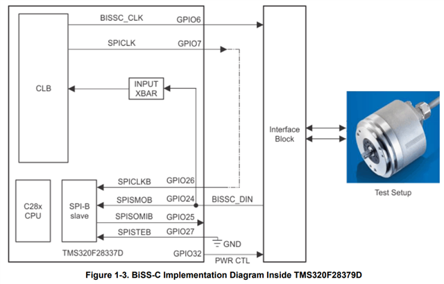
In that example (implemented on an F2837D, GPIO6 and GPIO7 are sourced from a CLB.
Those two GPIO can be mapped to Output X-BAR but they are not mapped to CLB Output X-BAR.
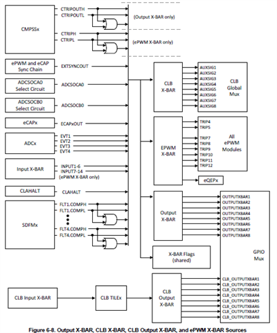
Seems to me since those are sourced from a CLB tile and per the diagram below, the GPIO selected should be mapped to CLB Output X-BAR.
But that's not what's done in the example so I'm unclear on how I should assign pins in my design. I'm not clear on how the BISSC_CLK and SPICLK (loop back signal) can be routed to the outside of the chip if not using CLB Output X-BAR. What am I missing?
Thanks!
Jason
