


Tool/software:
Hi, I have DAB hardware for which the following code is developed using EPWM modules at 100 kHz in an open loop. My primary bridge uses EPWM 4 and 5, whereas my secondary bridge uses EPWM 1 and 2. These EPWM modules cannot be changed as they are hard-wired in the PCB trace. I have used up counting because the primary should lead the secondary, and by updating the TBPHS register of modules 4 and 5, I can create a leading PWM in modules 4 and 5 with EPWM 1 as my master.
void Setup_ePWM(void)
{
    // Primary Bridge
    //ePWM 4 Configuration
    EPwm4Regs.TBCTL.bit.CLKDIV=0;//(Set clock division=00b) divide by 1
    EPwm4Regs.TBCTL.bit.HSPCLKDIV=0;//(Set high speed clock division=00b)divide by 1
    EPwm4Regs.TBCTL.bit.CTRMODE=0;//UP Mode
    EPwm4Regs.TBPRD=fs;//Period corresponding to 100kHz
    EPwm4Regs.CMPA.bit.CMPA =0.5*fs;//50% duty cycle
    EPwm4Regs.TBPHS.bit.TBPHS=PHI;//Set phase angle
    EPwm4Regs.TBCTL.bit.PHSEN=TB_ENABLE;//Set as a Slave
    EPwm4Regs.TBCTL.bit.SYNCOSEL=TB_SYNC_IN;// Input from master
    EPwm4Regs.AQCTLA.all=0x0024;//set high when TBCTR=CMPA Up and low when TBCTR=TBPRD
    EPwm4Regs.DBCTL.bit.OUT_MODE=DB_FULL_ENABLE;//Enable dead band module
    EPwm4Regs.DBCTL.bit.POLSEL=2;//Inverted signal at ePWM4B
    EPwm4Regs.DBFED.all=30;//30 block in FALLING EDGE
    EPwm4Regs.DBRED.all=30;//30 block in RISING EDGE

    //ePWM 5 configuration
    EPwm5Regs.TBCTL.bit.CLKDIV=0;//(Set clock division=01b) divide by 1
    EPwm5Regs.TBCTL.bit.HSPCLKDIV=0;//(Set high speed clock division=00b)divide by 1
    EPwm5Regs.TBCTL.bit.CTRMODE=0;//UP Mode
    EPwm5Regs.TBPRD=fs;//Period corresponding to 100kHz
    EPwm5Regs.CMPA.bit.CMPA =0.5*fs;//50% duty cycle
    EPwm5Regs.TBPHS.bit.TBPHS=PHI;//Set phase angle
    EPwm5Regs.TBCTL.bit.PHSEN=TB_ENABLE;//Set as a Slave
    EPwm5Regs.TBCTL.bit.SYNCOSEL=TB_SYNC_IN; // Input from master
    EPwm5Regs.AQCTLA.all=0x0012;// ;//set low when TBCTR=CMPA Up and high when TBCTR=TBPRD
    EPwm5Regs.DBCTL.bit.OUT_MODE=DB_FULL_ENABLE;//Enable dead band module
    EPwm5Regs.DBCTL.bit.POLSEL=2;//Inverted signal at ePWM5B
    EPwm5Regs.DBFED.all=30;//30 block in FALLING EDGE
    EPwm5Regs.DBRED.all=30;//30 block in RISING EDGE

    // Secondary Bridge
    //ePWM 1 Configuration
    EPwm1Regs.TBCTL.bit.CLKDIV=0;//(Set clock division=01b) divide by 1
    EPwm1Regs.TBCTL.bit.HSPCLKDIV=0;//(Set high speed clock division=00b)divide by 1
    EPwm1Regs.TBCTL.bit.CTRMODE=0;//Up Mode
    EPwm1Regs.TBPRD=fs;//Period corresponding to 100kHz
    EPwm1Regs.CMPA.bit.CMPA =0.5*fs;//50% duty cycle
    EPwm1Regs.TBPHS.bit.TBPHS=0;//Set phase angle of ePWM1 is 0
    EPwm1Regs.TBCTL.bit.PHSEN=TB_DISABLE;//Set as a Master
    EPwm1Regs.TBCTL.bit.SYNCOSEL=TB_CTR_ZERO;// synchronous output at CTR=0
    EPwm1Regs.AQCTLA.all=0x0024;//set high when TBCTR=CMPA Up and low when TBCTR=TBPRD
    EPwm1Regs.DBCTL.bit.OUT_MODE=DB_FULL_ENABLE;//Enable dead band module
    EPwm1Regs.DBCTL.bit.POLSEL=2;//Inverted signal at ePWM1B
    EPwm1Regs.DBFED.all=30;//30 block in FALLING EDGE
    EPwm1Regs.DBRED.all=30;//30 block in RISING EDGE

    //ePWM 2 configuration
    EPwm2Regs.TBCTL.bit.CLKDIV=0;//(Set clock division=01b) divide by 1
    EPwm2Regs.TBCTL.bit.HSPCLKDIV=0;//(Set high speed clock division=01b)divide by 1
    EPwm2Regs.TBCTL.bit.CTRMODE=0;//Up Mode
    EPwm2Regs.TBPRD=fs;//Period corresponding to 100kHz
    EPwm2Regs.CMPA.bit.CMPA =0.5*fs;//50% duty cycle
    EPwm2Regs.TBPHS.bit.TBPHS=0;//Set phase angle of ePWM5 is 180
    EPwm2Regs.TBCTL.bit.PHSEN=TB_ENABLE;//Set as a Slave
    EPwm2Regs.TBCTL.bit.SYNCOSEL=TB_SYNC_IN; // Input from master
    EPwm2Regs.AQCTLA.all=0x0012;//set low when TBCTR=CMPA Up and high when TBCTR=TBPRD
    EPwm2Regs.DBCTL.bit.OUT_MODE=DB_FULL_ENABLE;//Enable dead band module
    EPwm2Regs.DBCTL.bit.POLSEL=DB_ACTV_HIC;//Inverted signal at ePWM2B
    EPwm2Regs.DBFED.all=30;//50 block in FALLING EDGE
    EPwm2Regs.DBRED.all=30;//50 RISING EDGE

    //ePWM 3 interrupt configuration for ADC sampling
    EPwm3Regs.TBCTL.bit.CLKDIV=0;//(Set clock division=01b) divide by 1
    EPwm3Regs.TBCTL.bit.HSPCLKDIV=0;//(Set high speed clock division=00b)divide by 1
    EPwm3Regs.TBCTL.bit.CTRMODE=0;//Up Mode
    EPwm3Regs.TBPRD=0.5*fs;//Period corresponding to 200kHz
    EPwm3Regs.CMPA.bit.CMPA =0.25*fs;//50% duty cycle
    EPwm3Regs.ETSEL.bit.INTEN = 1; // Enable ePWM3 Interrupt generation
    EPwm3Regs.ETSEL.bit.INTSEL = 2; // Enable event time-base counter equal to CMPA when the timer is incrementing
    EPwm3Regs.ETPS.bit.INTPRD = 1; //Generate interrupt on 1st event

    EALLOW;
    EPwm3Regs.ETSEL.bit.SOCASEL = 2; // Generate SOCA event on ePWM3 timer = TBPRD
    EPwm3Regs.ETPS.bit.SOCAPRD = 1; // Generate SOCA on 1st event
    EPwm3Regs.ETSEL.bit.SOCAEN = 1; // Enable EPWMxSOCA pulse
    EPwm3Regs.ETCLR.bit.SOCA = 1;
    EDIS;
}
Now, I have to go for a peak current control using the following logic. This logic is working in PLECS simulation.
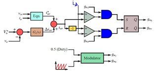
I have to access EPWM signals and use logic gates and flip-flops to implement this controller. Also, the Vo, Vin, Io, and Is signals are acquired using ADC pins. What should I write in the EPWM ISR function to make this controller work? This uses direct access to EPWM signals and uses a comparator, flipflop, and logic gates.
I don't expect entire coding from anyone. Little suggestions from here and there would help.
