


Other Parts Discussed in Thread: C2000WARE, UNIFLASH
Tool/software:
Hi experts,
I ask this for customer and I can use my LaunchPad to reproduce this issue.
Customer's test:
Customer use C:\ti\c2000\C2000Ware_5_02_00_00\driverlib\f28p55x\examples\dcsm\dcsm_security_tool.
dcsm.cmd is as below:
MEMORY
{
PAGE 0 :  /* Program Memory */

   /* Z1 OTP.  Z1 password locations / Flash and RAM partitioning */
   DCSM_OTP_Z1_LINKPOINTER     : origin = 0x78000, length = 0x00006
   DCSM_OTP_Z1_JLM_ENABLE      : origin = 0x78006, length = 0x00002
   DCSM_OTP_Z1_GPREG           : origin = 0x78008, length = 0x00008
   DCSM_OTP_Z1_PSWDLOCK        : origin = 0x78010, length = 0x00002
   DCSM_OTP_Z1_CRCLOCK         : origin = 0x78012, length = 0x00002
   DCSM_OTP_Z1_JTAG_PSWDH      : origin = 0x78014, length = 0x00004
   DCSM_OTP_Z1_CMAC_KEY        : origin = 0x78018, length = 0x00008

   /* DCSM Z1 Zone Select Contents (!!Movable!!) */
   DCSM_ZSEL_Z1_P0             : origin = 0x78020, length = 0x000020

   /* Z2 OTP.  Z2 password locations / Flash and RAM partitioning */
   DCSM_OTP_Z2_LINKPOINTER     : origin = 0x78200, length = 0x00006
   DCSM_OTP_Z2_RSVD            : origin = 0x78206, length = 0x00002
   DCSM_OTP_Z2_GPREG           : origin = 0x78208, length = 0x00008
   DCSM_OTP_Z2_PSWDLOCK        : origin = 0x78210, length = 0x00002
   DCSM_OTP_Z2_CRCLOCK         : origin = 0x78212, length = 0x00002
   DCSM_OTP_Z2_RSVD1           : origin = 0x78214, length = 0x0000C

   /* DCSM Z2 Zone Select Contents (!!Movable!!) */
   DCSM_ZSEL_Z2_P0             : origin = 0x78220, length = 0x000020

}

SECTIONS
{
   dcsm_otp_z1_linkpointer    : > DCSM_OTP_Z1_LINKPOINTER                 PAGE = 0
   dcsm_otp_z1_gpreg        : > DCSM_OTP_Z1_GPREG                        PAGE = 0, type = DSECT
   dcsm_otp_z1_pswdlock                  : > DCSM_OTP_Z1_PSWDLOCK                        PAGE = 0
   dcsm_otp_z1_crclock                      : > DCSM_OTP_Z1_CRCLOCK                                    PAGE = 0
   dcsm_otp_z1_jlm_enable   : > DCSM_OTP_Z1_JLM_ENABLE,     PAGE = 0
   dcsm_otp_z1_jtag_pswdh   : > DCSM_OTP_Z1_JTAG_PSWDH,     PAGE = 0, type = DSECT
   dcsm_otp_z1_cmac_key     : > DCSM_OTP_Z1_CMAC_KEY,       PAGE = 0, type = DSECT
   dcsm_zsel_z1                                               : > DCSM_ZSEL_Z1_P0                                                PAGE = 0

   dcsm_otp_z2_linkpointer    : > DCSM_OTP_Z2_LINKPOINTER                 PAGE = 0
   dcsm_otp_z2_gpreg        : > DCSM_OTP_Z2_GPREG                        PAGE = 0, type = DSECT
   dcsm_otp_z2_pswdlock                  : > DCSM_OTP_Z2_PSWDLOCK                        PAGE = 0, type = DSECT
   dcsm_otp_z2_crclock                      : > DCSM_OTP_Z2_CRCLOCK                                    PAGE = 0, type = DSECT
   dcsm_rsvd_z2             : > DCSM_OTP_Z2_RSVD,           PAGE = 0, type = DSECT
   dcsm_rsvd1_z2            : > DCSM_OTP_Z2_RSVD1,          PAGE = 0, type = DSECT
   dcsm_zsel_z2                                               : > DCSM_ZSEL_Z2_P0                                                PAGE = 0
}
dcsm.asm is as below:
;----------------------------------------------------------------------
; Zone 1
;----------------------------------------------------------------------
     .sect "dcsm_otp_z1_linkpointer"
      .retain
      .long 0x00003FFF
      .long 0x00003FFF
      .long 0x00003FFF

     .sect "dcsm_otp_z1_jlm_enable"
      .retain
      .long 0xFFFF000F     ;Z1OTP_JLM_ENABLE
;;     .sect "dcsm_otp_z1_jtag_pswdh"
;;      .retain
;;      .long 0x4BFFFFFF     ;Z1OTP_JTAGPSWDH0
;;      .long 0x3FFFFFFF     ;Z1OTP_JTAGPSWDH1
;;
;;     .sect "dcsm_otp_z1_cmac_key"
;;      .retain
;;      .long 0x00000000     ;Z1OTP_CMACKEY0
;;      .long 0x00000000     ;Z1OTP_CMACKEY1
;;      .long 0x00000000     ;Z1OTP_CMACKEY2
;;      .long 0x00000000     ;Z1OTP_CMACKEY3
;;
     .sect "dcsm_otp_z1_pswdlock"
      .retain
      .long 0xFB7FFFF0

     .sect "dcsm_otp_z1_crclock"
      .retain
      .long 0x7FFFFFFF

;;     .sect "dcsm_otp_z1_gpreg"
;;      .retain
;;      .long 0x5AFF1820     ;Z1OTP_GPREG1 = Z1_BOOTPIN
;;      .long 0x5Affffff     ;Z1OTP_GPREG2
;;      .long 0x00000000     ;Z1OTP_GPREG3 = Z1OTP_BOOTDEF_LOW
;;      .long 0xFFFFFFFF     ;Z1OTP_GPREG4 = Z1OTP_BOOTDEF_HIGH
     .sect "dcsm_zsel_z1"
      .retain
      .long 0x12345678     ;Z1OTP_CSMPSWD0 (LSW of 128-bit password)
      .long 0x00045678     ;Z1OTP_CSMPSWD1
      .long 0x12345678     ;Z1OTP_CSMPSWD2
      .long 0x3E1D5678     ;Z1OTP_CSMPSWD3 (MSW of 128-bit password)

      .long 0x55555555     ;Z1OTP_GRABSECT1
      .long 0x55555555     ;Z1OTP_GRABSECT2
      .long 0x00000155     ;Z1OTP_GRABSECT3
      .long 0x00055555     ;Z1OTP_GRABRAM1
      .long 0xFFFFFFFF     ;Reserved
      .long 0xFFFFFFFF     ;Reserved

      .long 0xFFFFFFFF     ;Z1OTP_EXEONLYSECT1
      .long 0x0000001F     ;Z1OTP_EXEONLYSECT2
      .long 0x000003FF     ;Z1OTP_EXEONLYRAM1
      .long 0xFFFFFFEF     ;Z1_DIAG
      .long 0xFFFFFFFF     ;Z1OTP_JTAGPSWDL0
      .long 0x2BFFFFFF     ;Z1OTP_JTAGPSWDL1


;----------------------------------------------------------------------

; For code security operation,after development has completed, prior to
; production, all other zone select block locations should be programmed
; to 0x0000 for maximum security.
; If the first zone select block at offset 0x10 is used, the section
; "dcsm_rsvd_z1" can be used to program these locations to 0x0000.
; This code is commented out for development.

;       .sect "dcsm_rsvd_z1"
;        .loop (1e0h)
;              .int 0x0000
;        .endloop


;----------------------------------------------------------------------
; Zone 2
;----------------------------------------------------------------------
     .sect "dcsm_otp_z2_linkpointer"
      .retain
      .long 0x00003FFF
      .long 0x00003FFF
      .long 0x00003FFF

;;     .sect "dcsm_rsvd_z2"
;;      .retain
;;      .long 0xFFFFFFFF     ;Reserved
;;     .sect "dcsm_otp_z2_pswdlock"
;;      .retain
;;      .long 0x1F7FFFFF

;;     .sect "dcsm_otp_z2_crclock"
;;      .retain
;;      .long 0x3FFFFFFF

;;     .sect "dcsm_otp_z2_gpreg"
;;      .retain
;;      .long 0x5AFF1820     ;Z2OTP_GPREG1 = Z2_BOOTPIN
;;      .long 0x5AFFFF13f     ;Z2OTP_GPREG2
;;      .long 0x00000000     ;Z2OTP_GPREG3 = Z2OTP_BOOTDEF_LOW
;;      .long 0xFFFFFFFF     ;Z2OTP_GPREG4 = Z2OTP_BOOTDEF_HIGH
;;     .sect "dcsm_rsvd1_z2"
;;      .retain
;;      .long 0xFFFFFFFF     ;Reserved
;;      .long 0xFFFFFFFF     ;Reserved

     .sect "dcsm_zsel_z2"
      .retain
      .long 0xFFFFFFFF     ;Z2OTP_CSMPSWD0 (LSW of 128-bit password)
      .long 0x1F7FFFFF     ;Z2OTP_CSMPSWD1
      .long 0xFFFFFFFF     ;Z2OTP_CSMPSWD2
      .long 0xFFFFFFFF     ;Z2OTP_CSMPSWD3 (MSW of 128-bit password)

      .long 0xAAAAAAAA     ;Z2OTP_GRABSECT1
      .long 0xAAAAAAAA     ;Z2OTP_GRABSECT2
      .long 0x000002AA     ;Z2OTP_GRABSECT3
      .long 0x000AAAAA     ;Z2OTP_GRABRAM1
      .long 0xFFFFFFFF     ;Reserved
      .long 0xFFFFFFFF     ;Reserved

      .long 0xFFFFFFFF     ;Z2OTP_EXEONLYSECT1
      .long 0x0000001F     ;Z2OTP_EXEONLYSECT2
      .long 0x000003FF     ;Z2OTP_EXEONLYRAM1
      .long 0xFFFFFFFF     ;Reserved
      .long 0xFFFFFFFF     ;Reserved
      .long 0xFFFFFFFF     ;Reserved


;----------------------------------------------------------------------

; For code security operation,after development has completed, prior to
; production, all other zone select block locations should be programmed
; to 0x0000 for maximum security.
; If the first zone select block at offset 0x10 is used, the section
; "dcsm_rsvd_z2" can be used to program these locations to 0x0000.
; This code is commented out for development.

;       .sect "dcsm_rsvd_z2"
;        .loop (1e0h)
;              .int 0x0000
;        .endloop


;----------------------------------------------------------------------
; End of file
;----------------------------------------------------------------------
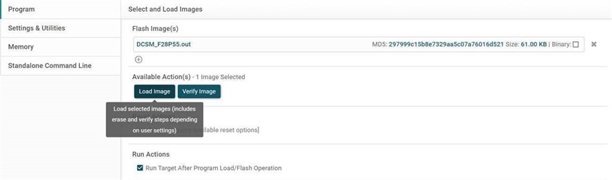
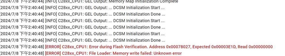
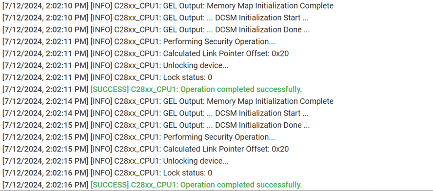
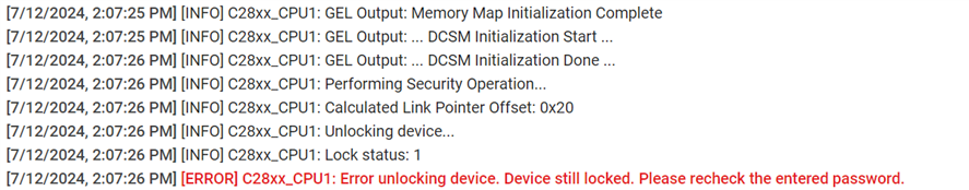
When customer load the .out file via Uniflash, it will shows error as below:
My test:
When I tested the same project on a new F28P55x Launchpad, there was also some issue, which was a little different from the customer's, but the project also could not be loaded correctly. The details are as follows:
1. I use the C2000ware example code and only modify Zone1 password0 to 0xFFFFFFFE. And set all RAM and FLASH secure in zone1.
when I load this .out via Uniflash, it it will shows error as below:
At this time, although it shows error, I can use this password to unlock zone1 and zone2 in uniflash.
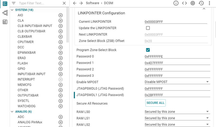
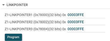
2. Then I modify zone1 password0 and JTAGPSWDL1 as below:
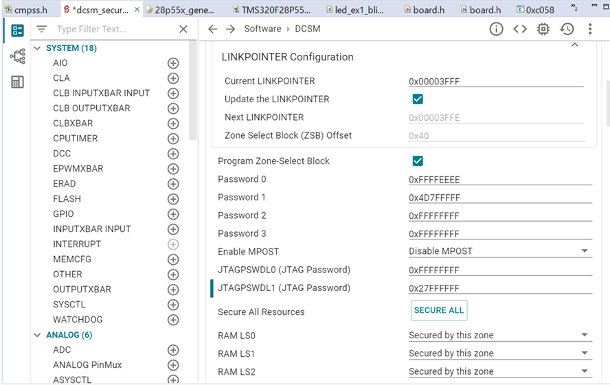
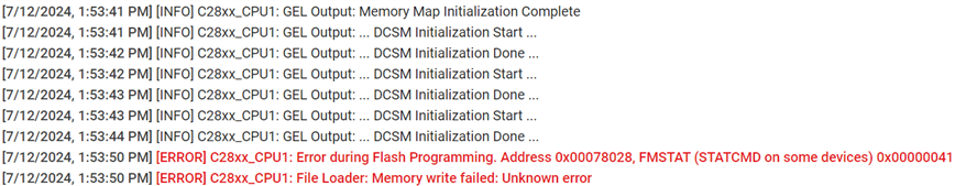
Then I use Uniflash to unlock, it shows that the password seems wrong.
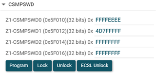
When I use ECSL unlock I can unlock and connect the device, it shows that the password0 is "0xFFFFFFFF". But when I use this password to unlock, it still shows the same error that the password is wrong.
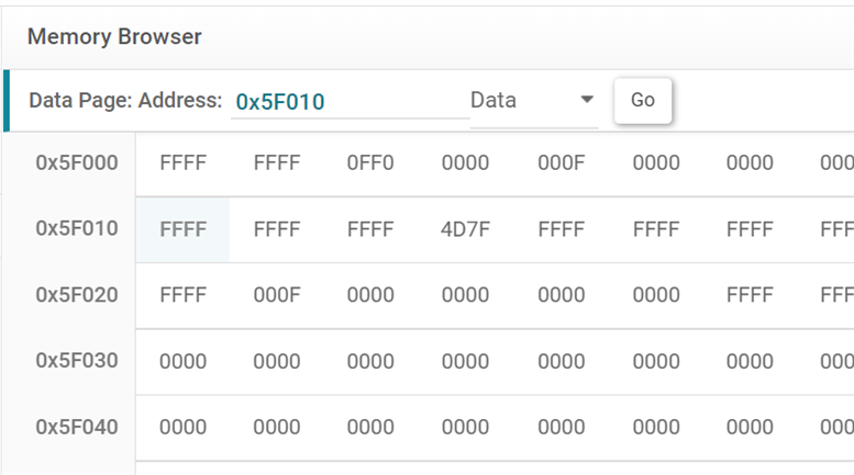
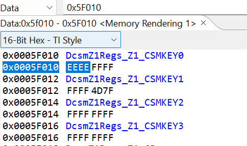
But when I use CCS ECSL unlock, in CCS I read the memory and the password0 is "0xFFFFEEEE"
Can you test it on your side? Why does it report an error? And how can I load DCSM successfully? Thank you!
Julia
