TMS320F28379D: Microcontroller Failures During First Power-Up

Part Number: TMS320F28379D
Other Parts Discussed in Thread: TMS320F28377D, TPS62420, TPS3702

Hello there,

I am currently using the 176-Pin TMS320F28377D in a design and have been experiencing catastrophic microcontroller failures during power-up of the circuit card assembly.  These failures occur intermittently, about one-third of the time.

I suspect that it may be related to the power supply topology I am using for VDDIO and VDD. My current configuration uses a cascading power architecture, where a 3.3 V buck regulator (VDDIO) feeds a second 1.2 V buck regulator (VDD). Because of this arrangement, there is a delay between the power-up of the two supply rails, ~2ms. The microcontroller is held in reset until the PGood of the regulators is high.

I am meeting the power sequencing requirements outlined in Section 6.9.1.2 and ensuring that VDD does not exceed VDDIO by more than 0.3 V. However, VDDOSC and VDD are not powering up at the same time.

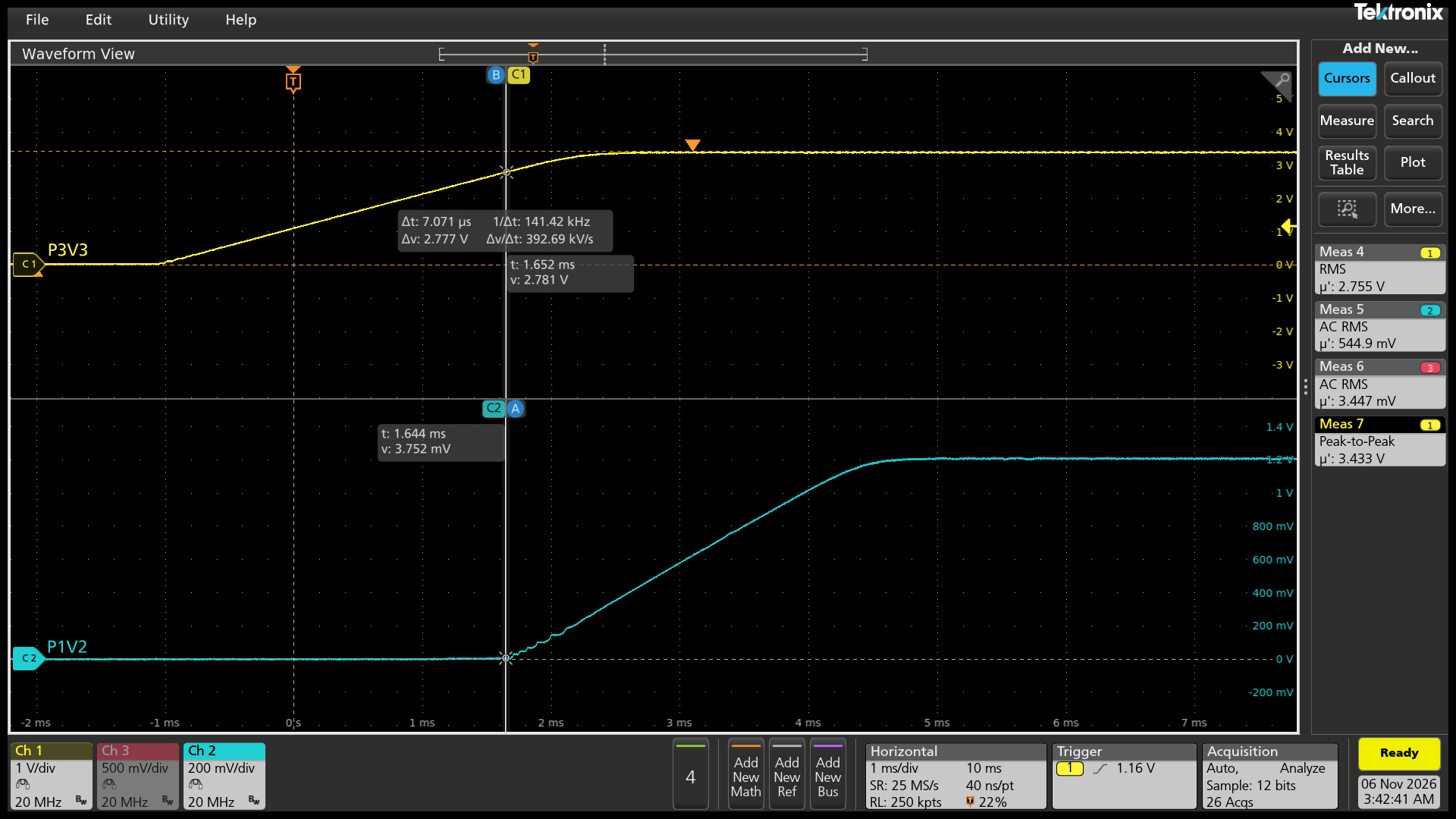
Could this delay in the power sequencing, or the fact that VDDOSC and VDD are not powering up simultaneously, be contributing to the intermittent failures? I've attached a couple of rise time capture between the 3.3 V and 1.2 V regulators. I would appreciate any insight into whether my current power topology or sequencing approach could be causing this issue.

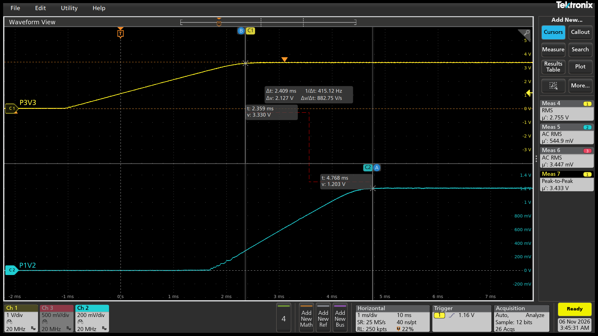
 

image.pngP1V2 v P3V3 Rise Time Setpoints.pngP1V2 Rise Time Difference 10nF.png

  • Hi Zachary,

    Your ~2 ms VDDIO→VDD delay is not a sequencing violation. The VDDOSC/VDD mismatch is a documented violation, but its known failure mode is clock drift — not catastrophic damage. Something else is likely destroying the parts, and your captures don't yet contain enough signals to identify it.


    1. The ~2 ms VDDIO-to-VDD delay is within spec

    Section 6.9.1.3 imposes a voltage-difference rule, not a timing rule: during ramp, VDD must not exceed VDDIO by more than 0.3 V. Both of your captures satisfy this comfortably — P3V3 is already at ~2.78 V before P1V2 leaves 0 V, and VDD never crosses VDDIO at any point.

    Your measured ramps also fit the other applicable limits:

    Requirement Spec Your captures
    VDD vs. VDDIO during ramp ≤ +0.3 V VDD always below VDDIO
    All supplies to full rail ≤ 10 ms Settled by ~4.7 ms
    Ramp rate per rail 330 V/s – 10⁵ V/s ~880 V/s measured

    There is no maximum timing-skew specification between the 3.3 V group and the 1.2 V VDD rail in the datasheet. We separately confirmed on E2E that VDDIO ramping ahead of VDD is acceptable, with the only hard rules being that VDD must never lead VDDIO and that ramp rates are met 3. We also characterizes the 0.3 V rule as less stringent during power-on/off transitions than at runtime.

    2. VDDOSC/VDD non-simultaneity is a real violation — with a non-destructive failure mode

    Section 6.9.1.3 and the silicon errata require VDDOSC and VDD to be powered on and off at the same time, and VDDOSC must never be powered while VDD is off. Since VDDOSC is part of the 3.3 V group that must track VDDIO within 0.3 V, your cascaded topology structurally guarantees this violation for ~2 ms every power-up.

    The documented consequence (errata SPRZ412N): VDDOSC powered without VDD causes an accumulating, persistent downward frequency drift in INTOSC1/INTOSC2, worse at high temperature, which can push the oscillator below its datasheet minimum and make a PLL clocked from INTOSC2 run unexpectedly slow.

    This explains intermittent, clock-dependent boot failures — it does not explain physically destroyed devices. Two important qualifiers:
    - If your design does not use INTOSC as a clock source, this requirement and errata can be disregarded entirely.
    - Your uploaded captures trace only P3V3 and P1V2. No VDDOSC trace is included, so simultaneity cannot be confirmed from the scope data — verify it separately on hardware.

    Our documented workarounds: keep VDDOSC and VDD powered together or use an external X1/X2 crystal as the PLL source, which has no VDDOSC/VDD-sequencing drift.

    3. Your topology is the sanctioned architecture — keep it, instrument it

    A cascading 3.3 V → 1.2 V design is required, not optional: the internal VREG is unsupported on this device, VREGENZ must be tied to VDDIO, and VDD must come from an external 1.2 V regulator. A missing external VDD supply was the confirmed root cause of an intermittent 1-in-20 power-on failure in one case.

    PGood/supervisor-gated reset is also a validated pattern. TI confirmed a dedicated supervisor monitoring VDDIO and driving XRS as a valid, robust approach in a resolved intermittent-failure case. Our own F28377D reference design (TIDUAD1A) uses a dual-output buck (TPS62420) with an RC-delayed enable to sequence 3.3 V before 1.2 V, a diode between outputs to hold VDDIO above VDD, and per-rail window supervisors (TPS3702) whose UV outputs are wire-OR'ed to the reset pin. Generating both rails from one controller is the cleanest way to shrink your VDDOSC/VDD skew without abandoning the architecture.


    Next diagnostic step — this is the gap blocking root-cause. We explicitly requires a single capture showing VDD, VDDIO, and XRSn simultaneously; two-signal captures were deemed insufficient to diagnose this class of fault. Add VDDOSC as a fourth trace. Specifically look for:
    - XRS release before rails are in regulation. If a supply lingers near the POR threshold, the device can issue periodic resets on XRS — check that no PGood threshold sits close to a POR/UV trip point.
    - Minimum-load behavior on the 1.2 V buck. An internal 12.8 mA source from VDD3VFL to VDD during flash activity can drive VDD to ~1.3 V if the regulator can't sink current; TI recommends an optional 82 Ω dummy load.
    - Power-down ordering. VDD exceeding VDDIO by >0.3 V forward-biases an internal ESD diode between rails; We recommend powering down VDD and VDDIO simultaneously, or VDD first. Your captures cover power-up only — if the failure is actually occurring at shutdown or during a brownout/retry, that is unmeasured.
    - Pre-power-up pin state. Section 6.9.1.1 requires digital pins not exceed VDDIO, and analog pins not exceed VDDA, by more than 0.3 V before power-up — a classic latch-up/damage path when an external interface powers before the CCA.


    Resources

    1. TMS320F2837xD Datasheet (SPRS880P), §6.9.1
    2. TMS320F2837xS Datasheet (SPRS881K)
    3. E2E: TMS320F28377D Inquiry About Power-Up Sequence
    4. E2E: Clarification on Power Sequencing Requirements and Tolerances
    5. TMS320F2837xD Silicon Errata (SPRZ412N), INTOSC Advisory
    6. E2E: Help Check Power On and Power Down Waveform
    7. TIDUAD1A Reference Design User Guide
    8. E2E: TMS320F28377D Powering Up and Down

    Best Regards,

    Zackary Fleenor

  • Hi Zackary,

    Thank you for such a detailed response! It provided a lot of helpful information and helped address some concerns we had regarding the VDDIO to VDD delay.

    We are currently using the device's internal oscillator. I can't say for certain, but I don't believe we've experienced any intermittent boot failures so far. But even if we haven't seen any yet, doesn't mean we won't in the future. We do have the option to use an external oscillator.

    I've attached a few scope captures that include our PGood signal, which we use to hold the microcontroller in reset. VDDA and VDDOSC are connected directly to our 3.3 V rail. 

    As for the failure mode, we've only seen it occur during the initial power-up as a short of the 1.2 V or 3.3 V rail. It has not been seen after a power down event. If the device powers up successfully, we haven't seen it occur again, even after multiple power cycles.

    Replacing the IC typically clears the short. We've only had two cases where a replacement IC failed again, both were on the same CCA. The third replacement of the IC was successful.

    Hopefully this additional information can help narrow down the root cause. It's definitely a head-scratcher. Thanks again for your help!

  • Hi Zachary,

    Glad we're able to help. Your captures show correct rail order and PGood gating, but P1V2 ramp rate is marginal and possibly below the 330 V/s minimum. Nothing we have ties a slow ramp to destructive shorts. The first-power-up-only, same-CCA pattern points more toward a board-level stressor, and no capture yet tests that.

    1. Captures vs. requirements

    Datasheet limits: ramp rate 330 to 10⁵ V/s on VDDIO, VDD, VDDA, VDD3VFL and VDDOSC. All supplies must reach full rail within 10 ms. VDD may be no more than 0.3 V above VDDIO during the ramp 1.

    Capture P1V2 start → regulation Measured slew Result
    A ~1.8 → ~4.7 ms 198.55 V/s (cursors: 1.091 V over 5.493 ms) Below 330 V/s if valid
    B ~1.4 → ~4.8 ms No cursor value ≈350 V/s from the stated times (my estimate)
    C ~1.8 → ~4.7 ms No cursor value ≈410 V/s from the stated times (my estimate)
    D ~1.68 → ~4.76 ms 354.35 V/s Passes, only ~7% above the minimum
    • Sequencing and reset: In all four, P1V2 stays below P3V3/VDDA. The 3.3 V rails settle in about 1.2–2.8 ms. All rails are in regulation under 10 ms. PGood stays low until P1V2 is near regulation.
    • Capture A caveat: The 198.55 V/s figure doesn't match A's own visible ramp window. 1.2 V over ~2.9 ms is about 410 V/s. The cursor span likely includes the soft-start foot or settling tail, so re-measure across the linear portion of the ramp.
    • Margin: Even the passing captures sit close to 330 V/s. Unit-to-unit and temperature variation could push some power-ups below it.
    • Slew spec: TI confirmed on E2E that the slew limits still apply, and that the 0.3 V rule is less stringent during power-on/off than at runtime 2.
    • VDDOSC: VDDOSC is on the 3.3 V rail and is not captured. It therefore powers ~2 ms before VDD. The datasheet requires them to power on and off together 1. The documented consequence is INTOSC frequency drift, not damage 3.

    2. What the failure pattern suggests

    • Slow ramp as the cause: This is unconfirmed. The retrieved datasheet and errata state the ramp limit, but none link a sub-330 V/s ramp to rail shorts or latch-up.
    • Supervision threshold: The datasheet notes that a supply held near the POR threshold can cause periodic resets on XRS 1. That is a reset symptom, not a short. Your captures show PGood, not XRS.
    • Internal VREG during ramp: The errata state the internal VREG is active during VDDIO power-up until VDD reaches ~0.7 V, and that this does not impact operation 4.
    • Pre-power pin state: Damage that occurs only at first power-up fits the pre-power pin rule. No digital pin may exceed VDDIO by more than 0.3 V, and no analog pin (including VREFHI) may exceed VDDA by more than 0.3 V, before power is applied 1. An E2E case showed 2.5 V appearing on an unpowered VDDA through internal ESD diode paths when only the digital supplies were on 5.
    • Same-CCA repeats: Two replacement failures on one CCA, then success, suggest a stressor tied to that board or its connected hardware. This is my inference, not a retrieved finding.
    • Open items: Pin states before power-up, the XRS pin itself, and inrush or short current at the moment of failure are all unmeasured.

    3. Recommended next steps

    1. Check pin voltages before power-up. Verify nothing drives MCU digital pins above VDDIO+0.3 V, or analog pins and VREFHI above VDDA+0.3 V, while the CCA is unpowered or ramping. Look at the JTAG emulator, connectors, other boards, and any reference that powers first.
    2. Capture a failing event.
      • Single-shot VDDIO, VDD, VDDOSC and XRS together. This is the capture TI previously asked for on a similar intermittent failure 6.
      • Add a current probe on the 3.3 V and 1.2 V inputs if you can. That shows which rail collapses first and when.
    3. Fix the P1V2 ramp margin. Re-measure on the linear portion across many units and temperatures. If it is below or near 330 V/s, speed it up. Keep it under 10⁵ V/s.
    4. Remove the VDDOSC/VDD violation. Since you use INTOSC and have an external oscillator option, use an X1/X2 crystal as the PLL source. Errata workarounds: power VDDOSC and VDD together, or use the crystal, which has no sequencing-related drift 3. Neither is expected to cure the shorts.
    5. Check 1.2 V buck minimum load. An internal 12.8 mA source can lift VDD to ~1.3 V in low-activity states. An optional 82 Ω load addresses this 1.
    6. Triage the failed parts and the bad CCA. Record which rail shorts on each failed part. Compare that CCA against good ones for anything that differs, such as connected harnesses, test fixtures, or assembly.

    1. TMS320F2837xD Datasheet (SPRS880P), §6.9.1
    2. E2E: Clarification on Power Sequencing Requirements and Tolerances
    3. Silicon Errata SPRZ412N, INTOSC advisory
    4. Silicon Errata SPRZ412N, VREG/XRS power-up advisories
    5. E2E: VDDA and VDD isolation
    6. E2E: Help check power on and power down waveform

    Best Regards,

    Zackary Fleenor