This thread has been locked.
If you have a related question, please click the "Ask a related question" button in the top right corner. The newly created question will be automatically linked to this question.
Hi all,
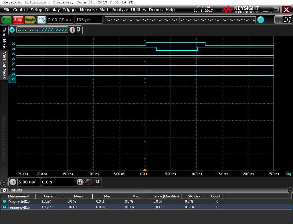
I am using the 28377S to implement the modulator/average current mode loop for a 4 phase interleaved converter. Everything is working okay except for when I drive extremely low duty cycles. As I continue to lower the duty cycle, eventually the EPWMxA waveforms are always low and a narrow pulse on the EPWMxB waveform appears. Eventually the pulse on EPWM1xB goes away, and then the other EPWMxB pulses go away which I would expect, but once the other pulses disappear at 0 duty cycle the pulse on EPWM1B returns. I found this to be very strange. If anyone can point me in the right direction as to how to fix it that would be useful. I've attached my configuration code for the EPWM modules below.
Best regards,
Lance Hummel
void Init_EPWM(void) { // // Setup TBCLK // //NOTE: The EPWM module for this processor has a built in hardware limitation on clock frequency of 60MHz to 100MHz for full functionality. //To handle this, an integer /2 of the main CPU clock is enabled by default in the register ClkCfgRegs.PERCLKDIVSEL.bit.EPWMCLKDIV EPwm1Regs.TBCTL.bit.CTRMODE = TB_COUNT_UPDOWN; // Count up-down EPwm1Regs.TBPRD = EPWM_COUNT_PERIOD; // Set timer period EPwm1Regs.TBCTL.bit.PHSEN = TB_DISABLE; // Disable phase loading EPwm1Regs.TBCTL.bit.SYNCOSEL = TB_CTR_ZERO;// Used as sync signal for phase locked PWMs EPwm1Regs.TBPHS.bit.TBPHS = 0x0000; // Phase is 0 EPwm1Regs.TBCTR = 0x0000; // Clear counter EPwm1Regs.TBCTL.bit.HSPCLKDIV = TB_DIV1; // Clock ratio to SYSCLKOUT EPwm1Regs.TBCTL.bit.CLKDIV = TB_DIV1; // // Setup shadow register load on ZERO // EPwm1Regs.CMPCTL.bit.SHDWAMODE = CC_SHADOW; EPwm1Regs.CMPCTL.bit.SHDWBMODE = CC_SHADOW; EPwm1Regs.CMPCTL.bit.LOADAMODE = CC_CTR_ZERO; EPwm1Regs.CMPCTL.bit.LOADBMODE = CC_CTR_ZERO; // // Set Compare values // EPwm1Regs.CMPA.bit.CMPA = 0; // Set compare A value EPwm1Regs.CMPB.bit.CMPB = EPWM_INTERRUPT_COUNT; // Set Compare B value // // Set actions // EPwm1Regs.AQCTLA.bit.CAU = AQ_CLEAR; // Set PWM1A on Zero EPwm1Regs.AQCTLA.bit.CAD = AQ_SET; // Clear PWM1A on event A, // up count //EPwm1Regs.AQCTLB.bit.CAU = AQ_SET; // Set PWM1B on Zero //EPwm1Regs.AQCTLB.bit.CAD = AQ_CLEAR; // Clear PWM1B on event B, // up count // // Setup Deadband (assumes non-inverted gate drive signals and EPWMxA as the source for both delays) // EPwm1Regs.DBCTL.bit.OUT_MODE = DB_FULL_ENABLE; EPwm1Regs.DBCTL.bit.POLSEL = DB_ACTV_HIC; EPwm1Regs.DBCTL.bit.IN_MODE = DBA_ALL; EPwm1Regs.DBRED.bit.DBRED = 0x00A; //100MHz EPWMCLK => 10ns per count, assume 100ns dead band to start EPwm1Regs.DBFED.bit.DBFED = 0x00A; //100MHz EPWMCLK => 10ns per count, assume 100ns dead band to start // // Interrupt where we will change the Compare Values // EPwm1Regs.ETSEL.bit.INTSEL = ET_CTRD_CMPB; // Select INT on CMPB down count EPwm1Regs.ETSEL.bit.INTEN = 1; // Enable INT EPwm1Regs.ETPS.bit.INTPRD = ET_1ST; // Generate INT on 1st event // // Configure ADC SOCA signal // EPwm1Regs.ETSEL.bit.SOCASEL = ET_CTR_PRD; EPwm1Regs.ETSEL.bit.SOCAEN = 1; EPwm1Regs.ETPS.bit.SOCAPRD = ET_1ST; // //Configure High-Resolution PWM Registers // EALLOW; EPwm1Regs.HRCNFG.all = 0x0; EPwm1Regs.HRCNFG.bit.EDGMODE = HR_BEP; EPwm1Regs.HRCNFG.bit.CTLMODE = HR_CMP; EPwm1Regs.HRCNFG.bit.HRLOAD = HR_CTR_ZERO; //EPwm1Regs.HRCNFG.bit.EDGMODEB = HR_BEP; //EPwm1Regs.HRCNFG.bit.CTLMODEB = HR_CMP; //EPwm1Regs.HRCNFG.bit.HRLOADB = HR_CTR_ZERO_PRD; EPwm1Regs.HRCNFG.bit.AUTOCONV = 0; EPwm1Regs.HRPCTL.bit.TBPHSHRLOADE = 1; EPwm1Regs.HRPCTL.bit.HRPE = 1; EDIS; // // Configure Trip-Zone Module Registers // /*EALLOW; EPwm1Regs.TZSEL.bit.OSHT1 = TZ_ENABLE; EPwm1Regs.TZCTL.bit.TZA = TZ_FORCE_LO; EPwm1Regs.TZCTL.bit.TZB = TZ_FORCE_LO; EDIS;*/ // // Setup TBCLK // //NOTE: The EPWM module for this processor has a built in hardware limitation on clock frequency of 60MHz to 100MHz for full functionality. //To handle this, an integer /2 of the main CPU clock is enabled by default in the register ClkCfgRegs.PERCLKDIVSEL.bit.EPWMCLKDIV EPwm2Regs.TBCTL.bit.CTRMODE = TB_COUNT_UPDOWN; // Count up-down EPwm2Regs.TBPRD = EPWM_COUNT_PERIOD; // Set timer period EPwm2Regs.TBCTL.bit.PHSEN = TB_ENABLE; // Enable phase loading EPwm2Regs.TBCTL.bit.SYNCOSEL = TB_SYNC_IN;// Pass on sync signal from master EPwm2Regs.TBPHS.bit.TBPHS = EPWM_PHASE_OFFSET_1; // Phase is 90 degrees EPwm2Regs.TBCTR = 0x0000; // Clear counter EPwm2Regs.TBCTL.bit.HSPCLKDIV = TB_DIV1; // Clock ratio to SYSCLKOUT EPwm2Regs.TBCTL.bit.CLKDIV = TB_DIV1; // // Setup shadow register load on ZERO // EPwm2Regs.CMPCTL.bit.SHDWAMODE = CC_SHADOW; EPwm2Regs.CMPCTL.bit.SHDWBMODE = CC_SHADOW; EPwm2Regs.CMPCTL.bit.LOADAMODE = CC_CTR_ZERO; EPwm2Regs.CMPCTL.bit.LOADBMODE = CC_CTR_ZERO; // // Set Compare values // EPwm2Regs.CMPA.bit.CMPA = 0; // Set compare A value EPwm2Regs.CMPB.bit.CMPB = EPWM_INTERRUPT_COUNT; // Set Compare B value // // Set actions // EPwm2Regs.AQCTLA.bit.CAU = AQ_CLEAR; // Set PWM1A on Zero EPwm2Regs.AQCTLA.bit.CAD = AQ_SET; // Clear PWM1A on event A, // up count //EPwm2Regs.AQCTLB.bit.CAU = AQ_SET; // Set PWM1B on Zero //EPwm2Regs.AQCTLB.bit.CAD = AQ_CLEAR; // Clear PWM1B on event B, // up count // // Setup Deadband (assumes non-inverted gate drive signals and EPWMxA as the source for both delays) // EPwm2Regs.DBCTL.bit.OUT_MODE = DB_FULL_ENABLE; EPwm2Regs.DBCTL.bit.POLSEL = DB_ACTV_HIC; EPwm2Regs.DBCTL.bit.IN_MODE = DBA_ALL; EPwm2Regs.DBRED.bit.DBRED = 0x00A; //100MHz EPWMCLK => 10ns per count, assume 100ns dead band to start EPwm2Regs.DBFED.bit.DBFED = 0x00A; //100MHz EPWMCLK => 10ns per count, assume 100ns dead band to start // // Interrupt where we will change the Compare Values // EPwm2Regs.ETSEL.bit.INTSEL = ET_CTRD_CMPB; // Select INT on CMPB down count EPwm2Regs.ETSEL.bit.INTEN = 1; // Enable INT EPwm2Regs.ETPS.bit.INTPRD = ET_1ST; // Generate INT on 1st event // // Configure ADC SOCA signal // EPwm2Regs.ETSEL.bit.SOCASEL = ET_CTR_PRD; EPwm2Regs.ETSEL.bit.SOCAEN = 1; EPwm2Regs.ETPS.bit.SOCAPRD = ET_1ST; // //Configure High-Resolution PWM Registers // EALLOW; EPwm2Regs.HRCNFG.all = 0x0; EPwm2Regs.HRCNFG.bit.EDGMODE = HR_BEP; EPwm2Regs.HRCNFG.bit.CTLMODE = HR_CMP; EPwm2Regs.HRCNFG.bit.HRLOAD = HR_CTR_ZERO; //EPwm2Regs.HRCNFG.bit.EDGMODEB = HR_BEP; //EPwm2Regs.HRCNFG.bit.CTLMODEB = HR_CMP; // EPwm2Regs.HRCNFG.bit.HRLOADB = HR_CTR_ZERO_PRD; EPwm2Regs.HRCNFG.bit.AUTOCONV = 0; EPwm2Regs.HRPCTL.bit.TBPHSHRLOADE = 1; EPwm2Regs.HRPCTL.bit.HRPE = 1; EDIS; // // Configure Trip-Zone Module Registers // /*EALLOW; EPwm2Regs.TZSEL.bit.OSHT1 = TZ_ENABLE; EPwm2Regs.TZCTL.bit.TZA = TZ_FORCE_LO; EPwm2Regs.TZCTL.bit.TZB = TZ_FORCE_LO; EDIS;*/ // // Setup TBCLK // //NOTE: The EPWM module for this processor has a built in hardware limitation on clock frequency of 60MHz to 100MHz for full functionality. //To handle this, an integer /2 of the main CPU clock is enabled by default in the register ClkCfgRegs.PERCLKDIVSEL.bit.EPWMCLKDIV EPwm3Regs.TBCTL.bit.CTRMODE = TB_COUNT_UPDOWN; // Count up-down EPwm3Regs.TBPRD = EPWM_COUNT_PERIOD; // Set timer period EPwm3Regs.TBCTL.bit.PHSEN = TB_ENABLE; // Enable phase loading EPwm3Regs.TBCTL.bit.SYNCOSEL = TB_SYNC_IN;// Pass on sync signal from master EPwm3Regs.TBPHS.bit.TBPHS = EPWM_PHASE_OFFSET_2; // Phase is 180 degrees EPwm3Regs.TBCTR = 0x0000; // Clear counter EPwm3Regs.TBCTL.bit.HSPCLKDIV = TB_DIV1; // Clock ratio to SYSCLKOUT EPwm3Regs.TBCTL.bit.CLKDIV = TB_DIV1; // // Setup shadow register load on ZERO // EPwm3Regs.CMPCTL.bit.SHDWAMODE = CC_SHADOW; EPwm3Regs.CMPCTL.bit.SHDWBMODE = CC_SHADOW; EPwm3Regs.CMPCTL.bit.LOADAMODE = CC_CTR_ZERO; EPwm3Regs.CMPCTL.bit.LOADBMODE = CC_CTR_ZERO; // // Set Compare values // EPwm3Regs.CMPA.bit.CMPA = 0; // Set compare A value EPwm3Regs.CMPB.bit.CMPB = EPWM_INTERRUPT_COUNT; // Set Compare B value // // Set actions // EPwm3Regs.AQCTLA.bit.CAU = AQ_CLEAR; // Set PWM1A on Zero EPwm3Regs.AQCTLA.bit.CAD = AQ_SET; // Clear PWM1A on event A, // up count //EPwm3Regs.AQCTLB.bit.CAU = AQ_SET; // Set PWM1B on Zero //EPwm3Regs.AQCTLB.bit.CAD = AQ_CLEAR; // Clear PWM1B on event B, // up count // // Setup Deadband (assumes non-inverted gate drive signals and EPWMxA as the source for both delays) // EPwm3Regs.DBCTL.bit.OUT_MODE = DB_FULL_ENABLE; EPwm3Regs.DBCTL.bit.POLSEL = DB_ACTV_HIC; EPwm3Regs.DBCTL.bit.IN_MODE = DBA_ALL; EPwm3Regs.DBRED.bit.DBRED = 0x00A; //100MHz EPWMCLK => 10ns per count, assume 100ns dead band to start EPwm3Regs.DBFED.bit.DBFED = 0x00A; //100MHz EPWMCLK => 10ns per count, assume 100ns dead band to start // // Interrupt where we will change the Compare Values // EPwm3Regs.ETSEL.bit.INTSEL = ET_CTRD_CMPB; // Select INT on CMPB down count EPwm3Regs.ETSEL.bit.INTEN = 1; // Enable INT EPwm3Regs.ETPS.bit.INTPRD = ET_1ST; // Generate INT on 1st event // // Configure ADC SOCA signal // EPwm3Regs.ETSEL.bit.SOCASEL = ET_CTR_PRD; EPwm3Regs.ETSEL.bit.SOCAEN = 1; EPwm3Regs.ETPS.bit.SOCAPRD = ET_1ST; // //Configure High-Resolution PWM Registers // EALLOW; EPwm3Regs.HRCNFG.all = 0x0; EPwm3Regs.HRCNFG.bit.EDGMODE = HR_BEP; EPwm3Regs.HRCNFG.bit.CTLMODE = HR_CMP; EPwm3Regs.HRCNFG.bit.HRLOAD = HR_CTR_ZERO; //EPwm3Regs.HRCNFG.bit.EDGMODEB = HR_BEP; //EPwm3Regs.HRCNFG.bit.CTLMODEB = HR_CMP; //EPwm3Regs.HRCNFG.bit.HRLOADB = HR_CTR_ZERO_PRD; EPwm3Regs.HRCNFG.bit.AUTOCONV = 0; EPwm3Regs.HRPCTL.bit.TBPHSHRLOADE = 1; EPwm3Regs.HRPCTL.bit.HRPE = 1; EDIS; // // Configure Trip-Zone Module Registers // /*EALLOW; EPwm3Regs.TZSEL.bit.OSHT1 = TZ_ENABLE; EPwm3Regs.TZCTL.bit.TZA = TZ_FORCE_LO; EPwm3Regs.TZCTL.bit.TZB = TZ_FORCE_LO; EDIS;*/ // // Setup TBCLK // //NOTE: The EPWM module for this processor has a built in hardware limitation on clock frequency of 60MHz to 100MHz for full functionality. //To handle this, an integer /2 of the main CPU clock is enabled by default in the register ClkCfgRegs.PERCLKDIVSEL.bit.EPWMCLKDIV EPwm4Regs.TBCTL.bit.CTRMODE = TB_COUNT_UPDOWN; // Count up-down EPwm4Regs.TBPRD = EPWM_COUNT_PERIOD; // Set timer period EPwm4Regs.TBCTL.bit.PHSEN = TB_ENABLE; // Enable phase loading EPwm4Regs.TBCTL.bit.PHSDIR = TB_UP; // Count down to achieve 270 degree phase shift EPwm4Regs.TBCTL.bit.SYNCOSEL = TB_SYNC_IN;// Pass on sync signal from master EPwm4Regs.TBPHS.bit.TBPHS = EPWM_PHASE_OFFSET_3; // Phase is 270 degrees (Note: Reversed count direction i.e. 360-90=270 degrees) EPwm4Regs.TBCTR = 0x0000; // Clear counter EPwm4Regs.TBCTL.bit.HSPCLKDIV = TB_DIV1; // Clock ratio to SYSCLKOUT EPwm4Regs.TBCTL.bit.CLKDIV = TB_DIV1; // // Setup shadow register load on ZERO // EPwm4Regs.CMPCTL.bit.SHDWAMODE = CC_SHADOW; EPwm4Regs.CMPCTL.bit.SHDWBMODE = CC_SHADOW; EPwm4Regs.CMPCTL.bit.LOADAMODE = CC_CTR_ZERO; EPwm4Regs.CMPCTL.bit.LOADBMODE = CC_CTR_ZERO; // // Set Compare values // EPwm4Regs.CMPA.bit.CMPA = 0; // Set compare A value EPwm4Regs.CMPB.bit.CMPB = EPWM_INTERRUPT_COUNT; // Set Compare B value // // Set actions // EPwm4Regs.AQCTLA.bit.CAU = AQ_CLEAR; // Set PWM1A on Zero EPwm4Regs.AQCTLA.bit.CAD = AQ_SET; // Clear PWM1A on event A, // up count //EPwm4Regs.AQCTLB.bit.CAU = AQ_SET; // Set PWM1B on Zero //EPwm4Regs.AQCTLB.bit.CAD = AQ_CLEAR; // Clear PWM1B on event B, // up count // // Setup Deadband (assumes non-inverted gate drive signals and EPWMxA as the source for both delays) // EPwm4Regs.DBCTL.bit.OUT_MODE = DB_FULL_ENABLE; EPwm4Regs.DBCTL.bit.POLSEL = DB_ACTV_HIC; EPwm4Regs.DBCTL.bit.IN_MODE = DBA_ALL; EPwm4Regs.DBRED.bit.DBRED = 0x00A; //100MHz EPWMCLK => 10ns per count, assume 100ns dead band to start EPwm4Regs.DBFED.bit.DBFED = 0x00A; //100MHz EPWMCLK => 10ns per count, assume 100ns dead band to start // // Interrupt where we will change the Compare Values // EPwm4Regs.ETSEL.bit.INTSEL = ET_CTRD_CMPB; // Select INT on CMPB down count EPwm4Regs.ETSEL.bit.INTEN = 1; // Enable INT EPwm4Regs.ETPS.bit.INTPRD = ET_1ST; // Generate INT on 1st event // // Configure ADC SOCA signal // EPwm4Regs.ETSEL.bit.SOCASEL = ET_CTR_PRD; EPwm4Regs.ETSEL.bit.SOCAEN = 1; EPwm4Regs.ETPS.bit.SOCAPRD = ET_1ST; // //Configure High-Resolution PWM Registers // EALLOW; EPwm4Regs.HRCNFG.all = 0x0; EPwm4Regs.HRCNFG.bit.EDGMODE = HR_BEP; EPwm4Regs.HRCNFG.bit.CTLMODE = HR_CMP; EPwm4Regs.HRCNFG.bit.HRLOAD = HR_CTR_ZERO; //EPwm4Regs.HRCNFG.bit.EDGMODEB = HR_BEP; //EPwm4Regs.HRCNFG.bit.CTLMODEB = HR_CMP; //EPwm4Regs.HRCNFG.bit.HRLOADB = HR_CTR_ZERO_PRD; EPwm4Regs.HRCNFG.bit.AUTOCONV = 0; EPwm4Regs.HRPCTL.bit.TBPHSHRLOADE = 1; EPwm4Regs.HRPCTL.bit.HRPE = 1; EDIS; // // Configure Trip-Zone Module Registers // /*EALLOW; EPwm4Regs.TZSEL.bit.OSHT1 = TZ_ENABLE; EPwm4Regs.TZCTL.bit.TZA = TZ_FORCE_LO; EPwm4Regs.TZCTL.bit.TZB = TZ_FORCE_LO; EDIS;*/ #if CLA_BENCHMARK //Setup TBCLK Registers EPwm5Regs.TBCTL.bit.CTRMODE = TB_COUNT_UP; EPwm5Regs.TBPRD = 0xFFFF; // Set timer period EPwm5Regs.TBCTL.bit.PHSEN = TB_DISABLE; // Enable phase loading EPwm5Regs.TBPHS.bit.TBPHS = 0x0000; // Phase is 0 degrees EPwm5Regs.TBCTL.bit.HSPCLKDIV = TB_DIV1; // Clock ratio to SYSCLKOUT EPwm5Regs.TBCTL.bit.CLKDIV = TB_DIV1; #endif }
Hi Lance,
I am sorry for the delay in replying.
I believe this behavior is a result of the dead-band configuration. When the duty is small enough that the dead-time is larger than the ON time, the pulses will disappear. By "a narrow pulse on the EPWMxB waveform", do you mean the xB output has a small low pulse but is close to full duty? If that is the case, then this is expected. If you mean that the xB output has a very small high pulse and is close to 0% duty, while the xA output is close to 0% duty as well, then this is a problem. Can you please clarify?
Assuming the first scenario above, if you don't like the small low pulses on the xB output, you could change the dead-time registers when ON time is less than dead-time. OR you could also generate xB separately through the action qualifier sub-module using CMPB. You can use CMPC/D for your interrupt generation.
I hope this helps.
Hrishi
Hrishi,
I switched over to directly controlling the dead band using the CMPB/CMPBHR registers to control the switching waveforms, but I'm still seeing the same issue on the EPWM1xA/xB channels. I still see these runt 10-20ns wide gate pulses with the duty cycle set to zero, and only on the EPWM1 output. EPWM2,3,4 are constant at zero duty cycle.
Here is my update code. I used the debugger to verify that the duty cycle is getting set to zero and it is. So I'm confused as to why I'm seeing anything happen on these EPWM outputs.
#include "master_include.h" void Init_EPWM(void) { // // Setup TBCLK // //NOTE: The EPWM module for this processor has a built in hardware limitation on clock frequency of 60MHz to 100MHz for full functionality. //To handle this, an integer /2 of the main CPU clock is enabled by default in the register ClkCfgRegs.PERCLKDIVSEL.bit.EPWMCLKDIV EPwm1Regs.TBCTL.bit.CTRMODE = TB_COUNT_UPDOWN; // Count up-down EPwm1Regs.TBPRD = EPWM_COUNT_PERIOD; // Set timer period EPwm1Regs.TBCTL.bit.PHSEN = TB_DISABLE; // Disable phase loading EPwm1Regs.TBCTL.bit.SYNCOSEL = TB_CTR_ZERO;// Used as sync signal for phase locked PWMs EPwm1Regs.TBPHS.bit.TBPHS = 0x0000; // Phase is 0 EPwm1Regs.TBCTR = 0x0000; // Clear counter EPwm1Regs.TBCTL.bit.HSPCLKDIV = TB_DIV1; // Clock ratio to SYSCLKOUT EPwm1Regs.TBCTL.bit.CLKDIV = TB_DIV1; // // Setup shadow register load on ZERO // EPwm1Regs.CMPCTL.bit.SHDWAMODE = CC_SHADOW; EPwm1Regs.CMPCTL.bit.SHDWBMODE = CC_SHADOW; EPwm1Regs.CMPCTL.bit.LOADAMODE = CC_CTR_ZERO; EPwm1Regs.CMPCTL.bit.LOADBMODE = CC_CTR_ZERO; // // Set Compare values // EPwm1Regs.CMPA.bit.CMPA = 0; // Set Compare A value EPwm1Regs.CMPB.bit.CMPB = 0; // Set Compare B value EPwm1Regs.CMPD = EPWM_INTERRUPT_COUNT; // Set Compare C value // // Set actions // EPwm1Regs.AQCTLA.bit.CAU = AQ_CLEAR; // Set PWM1A on Zero EPwm1Regs.AQCTLA.bit.CAD = AQ_SET; // Clear PWM1A on event A, // up count EPwm1Regs.AQCTLB.bit.CBU = AQ_SET; // Set PWM1B on Zero EPwm1Regs.AQCTLB.bit.CBD = AQ_CLEAR; // Clear PWM1B on event B, // up count // // Setup Deadband (assumes non-inverted gate drive signals and EPWMxA as the source for both delays) // /*EPwm1Regs.DBCTL.bit.OUT_MODE = DB_FULL_ENABLE; EPwm1Regs.DBCTL.bit.POLSEL = DB_ACTV_HIC; EPwm1Regs.DBCTL.bit.IN_MODE = DBA_ALL; EPwm1Regs.DBRED.bit.DBRED = 0x00A; //100MHz EPWMCLK => 10ns per count, assume 100ns dead band to start EPwm1Regs.DBFED.bit.DBFED = 0x00A; //100MHz EPWMCLK => 10ns per count, assume 100ns dead band to start*/ // // Interrupt where we will change the Compare Values // EPwm1Regs.ETSEL.bit.INTSELCMP = 1; // Select alternate compare source i.e. CMPC/CMPD EPwm1Regs.ETSEL.bit.INTSEL = ET_CTRD_CMPB; // Select INT on CMPD down count EPwm1Regs.ETSEL.bit.INTEN = 1; // Enable INT EPwm1Regs.ETPS.bit.INTPRD = ET_1ST; // Generate INT on 1st event // // Configure ADC SOCA signal // EPwm1Regs.ETSEL.bit.SOCASEL = ET_CTR_PRD; EPwm1Regs.ETSEL.bit.SOCAEN = 1; EPwm1Regs.ETPS.bit.SOCAPRD = ET_1ST; // //Configure High-Resolution PWM Registers // EALLOW; EPwm1Regs.HRCNFG.all = 0x0; EPwm1Regs.HRCNFG.bit.EDGMODE = HR_BEP; EPwm1Regs.HRCNFG.bit.CTLMODE = HR_CMP; EPwm1Regs.HRCNFG.bit.HRLOAD = HR_CTR_ZERO; EPwm1Regs.HRCNFG.bit.EDGMODEB = HR_BEP; EPwm1Regs.HRCNFG.bit.CTLMODEB = HR_CMP; EPwm1Regs.HRCNFG.bit.HRLOADB = HR_CTR_ZERO; EPwm1Regs.HRCNFG.bit.AUTOCONV = 0; EPwm1Regs.HRPCTL.bit.TBPHSHRLOADE = 1; EPwm1Regs.HRPCTL.bit.HRPE = 1; EDIS; // // Configure Trip-Zone Module Registers // /*EALLOW; EPwm1Regs.TZSEL.bit.OSHT1 = TZ_ENABLE; EPwm1Regs.TZCTL.bit.TZA = TZ_FORCE_LO; EPwm1Regs.TZCTL.bit.TZB = TZ_FORCE_LO; EDIS;*/ // // Setup TBCLK // //NOTE: The EPWM module for this processor has a built in hardware limitation on clock frequency of 60MHz to 100MHz for full functionality. //To handle this, an integer /2 of the main CPU clock is enabled by default in the register ClkCfgRegs.PERCLKDIVSEL.bit.EPWMCLKDIV EPwm2Regs.TBCTL.bit.CTRMODE = TB_COUNT_UPDOWN; // Count up-down EPwm2Regs.TBPRD = EPWM_COUNT_PERIOD; // Set timer period EPwm2Regs.TBCTL.bit.PHSEN = TB_ENABLE; // Enable phase loading EPwm2Regs.TBCTL.bit.SYNCOSEL = TB_SYNC_IN;// Pass on sync signal from master EPwm2Regs.TBPHS.bit.TBPHS = EPWM_PHASE_OFFSET_1; // Phase is 90 degrees EPwm2Regs.TBCTR = 0x0000; // Clear counter EPwm2Regs.TBCTL.bit.HSPCLKDIV = TB_DIV1; // Clock ratio to SYSCLKOUT EPwm2Regs.TBCTL.bit.CLKDIV = TB_DIV1; // // Setup shadow register load on ZERO // EPwm2Regs.CMPCTL.bit.SHDWAMODE = CC_SHADOW; EPwm2Regs.CMPCTL.bit.SHDWBMODE = CC_SHADOW; EPwm2Regs.CMPCTL.bit.LOADAMODE = CC_CTR_ZERO; EPwm2Regs.CMPCTL.bit.LOADBMODE = CC_CTR_ZERO; // // Set Compare values // EPwm2Regs.CMPA.bit.CMPA = 0; // Set compare A value EPwm2Regs.CMPB.bit.CMPB = 0; // Set Compare B value EPwm2Regs.CMPD = EPWM_INTERRUPT_COUNT; // // Set actions // EPwm2Regs.AQCTLA.bit.CAU = AQ_CLEAR; // Set PWM1A on Zero EPwm2Regs.AQCTLA.bit.CAD = AQ_SET; // Clear PWM1A on event A, // up count EPwm2Regs.AQCTLB.bit.CBU = AQ_SET; // Set PWM1B on Zero EPwm2Regs.AQCTLB.bit.CBD = AQ_CLEAR; // Clear PWM1B on event B, // up count // // Setup Deadband (assumes non-inverted gate drive signals and EPWMxA as the source for both delays) // /*EPwm2Regs.DBCTL.bit.OUT_MODE = DB_FULL_ENABLE; EPwm2Regs.DBCTL.bit.POLSEL = DB_ACTV_HIC; EPwm2Regs.DBCTL.bit.IN_MODE = DBA_ALL; EPwm2Regs.DBRED.bit.DBRED = 0x00A; //100MHz EPWMCLK => 10ns per count, assume 100ns dead band to start EPwm2Regs.DBFED.bit.DBFED = 0x00A; //100MHz EPWMCLK => 10ns per count, assume 100ns dead band to start*/ // // Interrupt where we will change the Compare Values // EPwm2Regs.ETSEL.bit.INTSELCMP = 1; EPwm2Regs.ETSEL.bit.INTSEL = ET_CTRD_CMPB; // Select INT on CMPD down count EPwm2Regs.ETSEL.bit.INTEN = 1; // Enable INT EPwm2Regs.ETPS.bit.INTPRD = ET_1ST; // Generate INT on 1st event // // Configure ADC SOCA signal // EPwm2Regs.ETSEL.bit.SOCASEL = ET_CTR_PRD; EPwm2Regs.ETSEL.bit.SOCAEN = 1; EPwm2Regs.ETPS.bit.SOCAPRD = ET_1ST; // //Configure High-Resolution PWM Registers // EALLOW; EPwm2Regs.HRCNFG.all = 0x0; EPwm2Regs.HRCNFG.bit.EDGMODE = HR_BEP; EPwm2Regs.HRCNFG.bit.CTLMODE = HR_CMP; EPwm2Regs.HRCNFG.bit.HRLOAD = HR_CTR_ZERO; EPwm2Regs.HRCNFG.bit.EDGMODEB = HR_BEP; EPwm2Regs.HRCNFG.bit.CTLMODEB = HR_CMP; EPwm2Regs.HRCNFG.bit.HRLOADB = HR_CTR_ZERO; EPwm2Regs.HRCNFG.bit.AUTOCONV = 0; EPwm2Regs.HRPCTL.bit.TBPHSHRLOADE = 1; EPwm2Regs.HRPCTL.bit.HRPE = 1; EDIS; // // Configure Trip-Zone Module Registers // /*EALLOW; EPwm2Regs.TZSEL.bit.OSHT1 = TZ_ENABLE; EPwm2Regs.TZCTL.bit.TZA = TZ_FORCE_LO; EPwm2Regs.TZCTL.bit.TZB = TZ_FORCE_LO; EDIS;*/ // // Setup TBCLK // //NOTE: The EPWM module for this processor has a built in hardware limitation on clock frequency of 60MHz to 100MHz for full functionality. //To handle this, an integer /2 of the main CPU clock is enabled by default in the register ClkCfgRegs.PERCLKDIVSEL.bit.EPWMCLKDIV EPwm3Regs.TBCTL.bit.CTRMODE = TB_COUNT_UPDOWN; // Count up-down EPwm3Regs.TBPRD = EPWM_COUNT_PERIOD; // Set timer period EPwm3Regs.TBCTL.bit.PHSEN = TB_ENABLE; // Enable phase loading EPwm3Regs.TBCTL.bit.SYNCOSEL = TB_SYNC_IN;// Pass on sync signal from master EPwm3Regs.TBPHS.bit.TBPHS = EPWM_PHASE_OFFSET_2; // Phase is 180 degrees EPwm3Regs.TBCTR = 0x0000; // Clear counter EPwm3Regs.TBCTL.bit.HSPCLKDIV = TB_DIV1; // Clock ratio to SYSCLKOUT EPwm3Regs.TBCTL.bit.CLKDIV = TB_DIV1; // // Setup shadow register load on ZERO // EPwm3Regs.CMPCTL.bit.SHDWAMODE = CC_SHADOW; EPwm3Regs.CMPCTL.bit.SHDWBMODE = CC_SHADOW; EPwm3Regs.CMPCTL.bit.LOADAMODE = CC_CTR_ZERO; EPwm3Regs.CMPCTL.bit.LOADBMODE = CC_CTR_ZERO; // // Set Compare values // EPwm3Regs.CMPA.bit.CMPA = 0; // Set compare A value EPwm3Regs.CMPB.bit.CMPB = 0; // Set Compare B value EPwm3Regs.CMPD = EPWM_INTERRUPT_COUNT; // // Set actions // EPwm3Regs.AQCTLA.bit.CAU = AQ_CLEAR; // Set PWM1A on Zero EPwm3Regs.AQCTLA.bit.CAD = AQ_SET; // Clear PWM1A on event A, // up count EPwm3Regs.AQCTLB.bit.CBU = AQ_SET; // Set PWM1B on Zero EPwm3Regs.AQCTLB.bit.CBD = AQ_CLEAR; // Clear PWM1B on event B, // up count // // Setup Deadband (assumes non-inverted gate drive signals and EPWMxA as the source for both delays) // /*EPwm3Regs.DBCTL.bit.OUT_MODE = DB_FULL_ENABLE; EPwm3Regs.DBCTL.bit.POLSEL = DB_ACTV_HIC; EPwm3Regs.DBCTL.bit.IN_MODE = DBA_ALL; EPwm3Regs.DBRED.bit.DBRED = 0x00A; //100MHz EPWMCLK => 10ns per count, assume 100ns dead band to start EPwm3Regs.DBFED.bit.DBFED = 0x00A; //100MHz EPWMCLK => 10ns per count, assume 100ns dead band to start*/ // // Interrupt where we will change the Compare Values // EPwm3Regs.ETSEL.bit.INTSELCMP = 1; EPwm3Regs.ETSEL.bit.INTSEL = ET_CTRD_CMPB; // Select INT on CMPD down count EPwm3Regs.ETSEL.bit.INTEN = 1; // Enable INT EPwm3Regs.ETPS.bit.INTPRD = ET_1ST; // Generate INT on 1st event // // Configure ADC SOCA signal // EPwm3Regs.ETSEL.bit.SOCASEL = ET_CTR_PRD; EPwm3Regs.ETSEL.bit.SOCAEN = 1; EPwm3Regs.ETPS.bit.SOCAPRD = ET_1ST; // //Configure High-Resolution PWM Registers // EALLOW; EPwm3Regs.HRCNFG.all = 0x0; EPwm3Regs.HRCNFG.bit.EDGMODE = HR_BEP; EPwm3Regs.HRCNFG.bit.CTLMODE = HR_CMP; EPwm3Regs.HRCNFG.bit.HRLOAD = HR_CTR_ZERO; EPwm3Regs.HRCNFG.bit.EDGMODEB = HR_BEP; EPwm3Regs.HRCNFG.bit.CTLMODEB = HR_CMP; EPwm3Regs.HRCNFG.bit.HRLOADB = HR_CTR_ZERO; EPwm3Regs.HRCNFG.bit.AUTOCONV = 0; EPwm3Regs.HRPCTL.bit.TBPHSHRLOADE = 1; EPwm3Regs.HRPCTL.bit.HRPE = 1; EDIS; // // Configure Trip-Zone Module Registers // /*EALLOW; EPwm3Regs.TZSEL.bit.OSHT1 = TZ_ENABLE; EPwm3Regs.TZCTL.bit.TZA = TZ_FORCE_LO; EPwm3Regs.TZCTL.bit.TZB = TZ_FORCE_LO; EDIS;*/ // // Setup TBCLK // //NOTE: The EPWM module for this processor has a built in hardware limitation on clock frequency of 60MHz to 100MHz for full functionality. //To handle this, an integer /2 of the main CPU clock is enabled by default in the register ClkCfgRegs.PERCLKDIVSEL.bit.EPWMCLKDIV EPwm4Regs.TBCTL.bit.CTRMODE = TB_COUNT_UPDOWN; // Count up-down EPwm4Regs.TBPRD = EPWM_COUNT_PERIOD; // Set timer period EPwm4Regs.TBCTL.bit.PHSEN = TB_ENABLE; // Enable phase loading EPwm4Regs.TBCTL.bit.PHSDIR = TB_UP; // Count down to achieve 270 degree phase shift EPwm4Regs.TBCTL.bit.SYNCOSEL = TB_SYNC_IN;// Pass on sync signal from master EPwm4Regs.TBPHS.bit.TBPHS = EPWM_PHASE_OFFSET_3; // Phase is 270 degrees (Note: Reversed count direction i.e. 360-90=270 degrees) EPwm4Regs.TBCTR = 0x0000; // Clear counter EPwm4Regs.TBCTL.bit.HSPCLKDIV = TB_DIV1; // Clock ratio to SYSCLKOUT EPwm4Regs.TBCTL.bit.CLKDIV = TB_DIV1; // // Setup shadow register load on ZERO // EPwm4Regs.CMPCTL.bit.SHDWAMODE = CC_SHADOW; EPwm4Regs.CMPCTL.bit.SHDWBMODE = CC_SHADOW; EPwm4Regs.CMPCTL.bit.LOADAMODE = CC_CTR_ZERO; EPwm4Regs.CMPCTL.bit.LOADBMODE = CC_CTR_ZERO; // // Set Compare values // EPwm4Regs.CMPA.bit.CMPA = 0; // Set compare A value EPwm4Regs.CMPB.bit.CMPB = 0; // Set Compare B value EPwm4Regs.CMPD = EPWM_INTERRUPT_COUNT; // // Set actions // EPwm4Regs.AQCTLA.bit.CAU = AQ_CLEAR; // Set PWM1A on Zero EPwm4Regs.AQCTLA.bit.CAD = AQ_SET; // Clear PWM1A on event A, // up count EPwm4Regs.AQCTLB.bit.CBU = AQ_SET; // Set PWM1B on Zero EPwm4Regs.AQCTLB.bit.CBD = AQ_CLEAR; // Clear PWM1B on event B, // up count // // Setup Deadband (assumes non-inverted gate drive signals and EPWMxA as the source for both delays) // /*EPwm4Regs.DBCTL.bit.OUT_MODE = DB_FULL_ENABLE; EPwm4Regs.DBCTL.bit.POLSEL = DB_ACTV_HIC; EPwm4Regs.DBCTL.bit.IN_MODE = DBA_ALL; EPwm4Regs.DBRED.bit.DBRED = 0x00A; //100MHz EPWMCLK => 10ns per count, assume 100ns dead band to start EPwm4Regs.DBFED.bit.DBFED = 0x00A; //100MHz EPWMCLK => 10ns per count, assume 100ns dead band to start*/ // // Interrupt where we will change the Compare Values // EPwm4Regs.ETSEL.bit.INTSELCMP = 1; EPwm4Regs.ETSEL.bit.INTSEL = ET_CTRD_CMPB; // Select INT on CMPD down count EPwm4Regs.ETSEL.bit.INTEN = 1; // Enable INT EPwm4Regs.ETPS.bit.INTPRD = ET_1ST; // Generate INT on 1st event // // Configure ADC SOCA signal // EPwm4Regs.ETSEL.bit.SOCASEL = ET_CTR_PRD; EPwm4Regs.ETSEL.bit.SOCAEN = 1; EPwm4Regs.ETPS.bit.SOCAPRD = ET_1ST; // //Configure High-Resolution PWM Registers // EALLOW; EPwm4Regs.HRCNFG.all = 0x0; EPwm4Regs.HRCNFG.bit.EDGMODE = HR_BEP; EPwm4Regs.HRCNFG.bit.CTLMODE = HR_CMP; EPwm4Regs.HRCNFG.bit.HRLOAD = HR_CTR_ZERO; EPwm4Regs.HRCNFG.bit.EDGMODEB = HR_BEP; EPwm4Regs.HRCNFG.bit.CTLMODEB = HR_CMP; EPwm4Regs.HRCNFG.bit.HRLOADB = HR_CTR_ZERO; EPwm4Regs.HRCNFG.bit.AUTOCONV = 0; EPwm4Regs.HRPCTL.bit.TBPHSHRLOADE = 1; EPwm4Regs.HRPCTL.bit.HRPE = 1; EDIS; // // Configure Trip-Zone Module Registers // /*EALLOW; EPwm4Regs.TZSEL.bit.OSHT1 = TZ_ENABLE; EPwm4Regs.TZCTL.bit.TZA = TZ_FORCE_LO; EPwm4Regs.TZCTL.bit.TZB = TZ_FORCE_LO; EDIS;*/ #if CLA_BENCHMARK //Setup TBCLK Registers EPwm5Regs.TBCTL.bit.CTRMODE = TB_COUNT_UP; EPwm5Regs.TBPRD = 0xFFFF; // Set timer period EPwm5Regs.TBCTL.bit.PHSEN = TB_DISABLE; // Enable phase loading EPwm5Regs.TBPHS.bit.TBPHS = 0x0000; // Phase is 0 degrees EPwm5Regs.TBCTL.bit.HSPCLKDIV = TB_DIV1; // Clock ratio to SYSCLKOUT EPwm5Regs.TBCTL.bit.CLKDIV = TB_DIV1; #endif }
Hi Lance,
What are the values of the CMPA and CMPB registers when you see these pulses? I am wondering if the values for these registers violate the duty cycle restriction when HRPWM is enabled i.e. these values cannot be < 3 or > (PRD-3).
Also, you have now disabled the dead-band module completely, correct?
Thanks.
Hrishi
Hrishi,
I am forcing the CMPA and CMPB registers to zero. Based on my EPWM configuration I would expect EPWM1A to be low all the time, and EPWM1B to be high all the time. I know that the HRPWM doesn't work below 3 PWMCLK counts, but I don't need the HRPWM to be working, I just need to be able to drive the duty cycle to the ideal zero. Below is the code I'm using to update the registers via a routine run in the CLA. The ON_OFF_READ macro is always false and forces the duty cycle to zero. So I know all the CMPA/B and CMPA/BHR are always set to zero. I also validated that in the debugger. Also the dead band module is disabled.
if(ON_OFF_READ == FALSE){ //If shut off, set duty cycle to zero duty1 = MIN_DUTY_CYCLE_SAT; } //Calculate number of counts to implement duty cycle PWM_COURSE_CNTS1 = (int)(EPWM_COUNT_PERIOD*duty1); //Set counts to implement the 100ns dead band PWM_COURSE_CNTS_DB1 = PWM_COURSE_CNTS1 + DB_OFFSET; if(PWM_COURSE_CNTS1 == 0){ PWM_COURSE_CNTS_DB1 = 0; //At zero duty cycle set the complement channel to match as well } //Calculate HRPWM number (use fractional intrinsic to save clock cycles) PWM_FINE_CNTS1 = ((int)(((PWM_CLK_TIME/HRPWM_CLK_TIME)*(__mfracf32(EPWM_COUNT_PERIOD*duty1))) + 0.5)) << 8; //Update CMPx/CMPxHR registers EPwm1Regs.CMPA.bit.CMPA = PWM_COURSE_CNTS1; EPwm1Regs.CMPA.bit.CMPAHR = PWM_FINE_CNTS1; EPwm1Regs.CMPB.bit.CMPB = PWM_COURSE_CNTS_DB1; EPwm1Regs.CMPB.bit.CMPBHR = PWM_FINE_CNTS1;
Lance
I was already doing that, with the CMPA/CMPB and the CMPA/BHR registers, and I made the change to HRLOAD and it didn't fix the issue I'm seeing on the EPWM1 outputs.
Lance,
This behavior is strange. We have reduced it down to a pretty straight-forward configuration and I do not expect any pulses at the output when CMPx:CMPxHR is 0.
I think you must have already checked but please make sure that dead-band is completely disabled. Also, make sure other AQ settings are set to 'don't care'.
If above look fine, the next thing to look at would be TZ registers. Make sure all TZCTL actions are set to 'do nothing', which is not the default.
Hrishi
Lance,
Have you seen this with multiple devices? Does the behavior improve if you disable HRPWM?
Thanks.
Hrishi
Lance,
Okay that's good. When you get to this mode where CMPA/B values are 0, in addition to making CMPAHR and CMPBHR 0 also make sure TBPRDHR is 0. If you do that, these pulses should go away even while HRPWM is enabled. You can then start using HRPWM again when the CMP values jump from 0 to 3.
Let me know how this goes.
Hrishi
Hrishi,
It happens every EPWM cycle. I'm already at the point where I don't have a lot of clock cycles to spare in terms of the control loop I'm running, so hopefully I can put in the ability to enable/disable the HRPE bit when appropriate and still hit the required ISR timing.
Lance