


We produce the PWM signals for a buck – boost stage with a PWM unit of the C2000 F28374 using the dead band module.
While testing the PWM operation in its extreme points (start / stop, 100% / 0% dutycycle, different dead band settings etc.) I discovered a for me none plausible behavior.
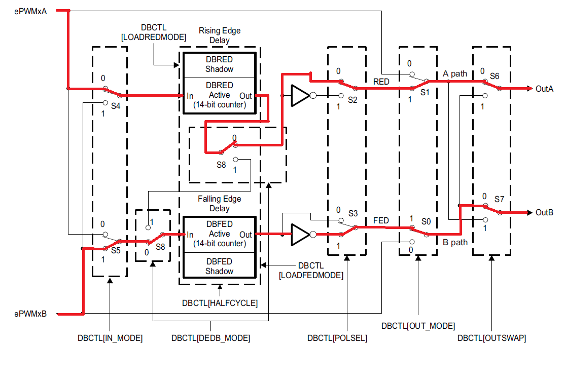
The PWM unit is configured in a way, that signal A and B have the same action qualifiers on CMPA while signal B gets inverted over the dead band module. RED can be applied to Signal A, FED to singal B.
In 0% duty cycle operation Signal A is high and signal B is low, vice versa in 100% duty cycle.
Changing the duty cycle to 0% while RED is 0 and then increasing RED to e.g. 100ns forces Output A to low. This only happens when RED has been 0 before the duty cycle change. That means that changing the duty cycle to 0 with RED = 100ns and then changing RED to 0 and back to 100ns works as expected (Output A stays high).
Same thing happens on Output B in 100% duty cycle operation when changing FED.

Of course using dead times for 100 or 0% duty cycle does not make sense and probably we never see this scenario as we have minimum allowed dead times so no one could set FED / RED to 0 in normal operation. Anyway my claim is understanding the configuration and the resulting behavior of the PWM unit to 100% in all theoretical possible operating conditions.
Are there any explanations for this behavior?
Below you can find our configuration routines:
Configuration of PWM unit:
void PWMConfigBooster(volatile struct EPWM_REGS *EPWM)
{
EPwm1Regs.TBCTL.bit.CTRMODE = TB_COUNT_UPDOWN; // Asymmetrical mode
EPwm1Regs.TBPRD = PWM_50KHZ_PRD_CNTUPDOWN; // Period = 900 TBCLK counts
EPwm1Regs.TBPHS.bit.TBPHS = 0; // Set Phase register to zero
EPwm1Regs.TBCTL.bit.PHSEN = TB_DISABLE; // disable phase sync as booster pwm is Master
EPwm1Regs.HRPCTL.bit.TBPHSHRLOADE = 0;
EPwm1Regs.TBCTL.bit.SYNCOSEL = TB_CTR_ZERO; // Sync out to all slaves
EPwm1Regs.TBCTL.bit.PHSDIR = 1; // count up after SYNC event and the new value of the phase (TBPHS) is loaded.
EPwm1Regs.TBPHS.bit.TBPHS = 0; // initial - coarse phase offset relative to ePWM1
EPwm1Regs.TBCTL.bit.PRDLD = TB_SHADOW;
EPwm1Regs.TBCTL.bit.HSPCLKDIV = TB_DIV1; // Prescaler = 1
EPwm1Regs.TBCTL.bit.CLKDIV = TB_DIV1; // TBCLK = SYSCLKOUT
EPwm1Regs.CMPCTL.bit.SHDWAMODE = CC_SHADOW;
EPwm1Regs.CMPCTL.bit.SHDWBMODE = CC_SHADOW;
EPwm1Regs.CMPCTL.bit.LOADAMODE = CC_CTR_ZERO; // load on CTR=Zero
EPwm1Regs.CMPCTL.bit.LOADBMODE = CC_CTR_ZERO; // load on CTR=Zero
StopBoosterPWM();
EPwm1Regs.AQCTL.bit.SHDWAQAMODE = 1; //enable shadow loading for action qualifier A register
EPwm1Regs.AQCTL.bit.SHDWAQBMODE = 1; //enable shadow loading for action qualifier B register
//configure deadband module to use rising edge delay on output A and to invert output B
//see DeadBandModuleConfigHssPwms.png for more details
EPwm1Regs.DBCTL.bit.IN_MODE = 0x2; // EPWMxA is the source for rising-edge delay, EPWMxB for falling-edge delay. (S4 = 0, S5 = 1)
EPwm1Regs.DBCTL.bit.DEDB_MODE = 0x0; // S8 = 0
EPwm1Regs.DBCTL.bit.POLSEL = 0x2; // invert ePWMxB signal coming out of falling edge delay block (S2 = 0, S3 = 1)
EPwm1Regs.DBCTL.bit.OUT_MODE = 0x3; // enable Dead-band module for EPWMxA and EPWMxB signals (S0 and S1 = 1)
EPwm1Regs.DBCTL.bit.OUTSWAP = 0x0; // S6 and S7 = 0
EPwm1Regs.DBFED.bit.DBFED = PWM_DEADTIME_IN_TICKS; // FED = 50 TBCLKs initially
EPwm1Regs.DBRED.bit.DBRED = PWM_DEADTIME_IN_TICKS; // RED = 50 TBCLKs initially
}
Function to stop PWM
void StopBoosterPWM(void)
{
#ifdef SET_HSS_PWM_STOP_GPIO
SET_HSS_PWM_STOP_GPIO
#endif
EPwm1Regs.AQCTLA.bit.CAU = AQ_CLEAR;
EPwm1Regs.AQCTLA.bit.CAD = AQ_CLEAR;
EPwm1Regs.AQCTLB.bit.CAU = AQ_SET; //signal gets inverted in the deadband module
EPwm1Regs.AQCTLB.bit.CAD = AQ_SET; //signal gets inverted in the deadband module
#ifdef CLEAR_HSS_PWM_START_GPIO
CLEAR_HSS_PWM_START_GPIO
#endif
}
Function to start PWM
void StartBoosterPWM(void)
{
#ifdef SET_HSS_PWM_STOP_GPIO
SET_HSS_PWM_STOP_GPIO
#endif
EPwm1Regs.AQCTLA.bit.CAU = AQ_CLEAR;
EPwm1Regs.AQCTLA.bit.CAD = AQ_SET;
EPwm1Regs.AQCTLB.bit.CAU = AQ_CLEAR; //signal gets inverted in the deadband module
EPwm1Regs.AQCTLB.bit.CAD = AQ_SET; //signal gets inverted in the deadband module
#ifdef CLEAR_HSS_PWM_STOP_GPIO
CLEAR_HSS_PWM_STOP_GPIO
#endif
}
Thanks!
Jens

