This thread has been locked.

If you have a related question, please click the "Ask a related question" button in the top right corner. The newly created question will be automatically linked to this question.

Inverter design reference file selection (TIDA01292 or TIDM-HV-1PH-DCAC)

Other Parts Discussed in Thread: TIDM-HV-1PH-DCAC, TIDA-01292, LM5101, LM5101B

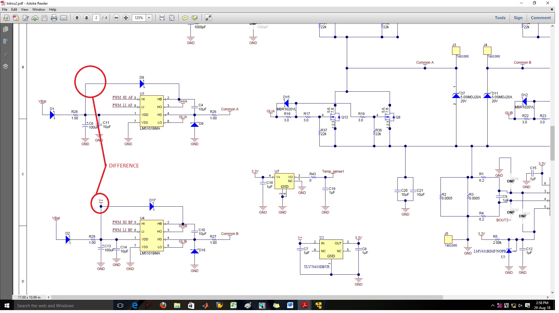
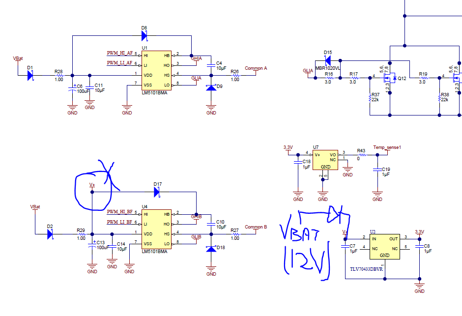
This is with reference to the inverter design reference file. Actually we
are looking for application with:

Input voltage - 48VDC
Ouput voltage - 60VAC RMS
Frequency- 50 to 60Hz
Power - 200 W
Pure Sinewave Inverter

upon surveying we came across 2 designs TIDA-01292 and TIDM-HV-1PH-DCAC,  which would be the best design suitable for our application after small modification.

  • Rajat,

    Please understand TI Designs are solving subsystem problem and not the end system, the intention is you will do you independent engineering evaluation before selecting some subystsms from the TI design for your system.

    TIDM-HV-1PH-DCAC has SW released in C2000Wars SDK.

    TIDA-01292 SW is not available.

    From a cost pespective TIDA-01292 will be better.

    From a performance perspective TIDM-HV-1PH-DCAC is better.

    I have also referrred this thread to the ownder of TIDA-01292 to comment / suggest.
  • Hi Rajat,

    As Manish mentioned, we don't have the firmware for TIDA-01292 released on web since the main intention of doing this design was to showcase the performance of TI's SMD MOSFETs in low frequency inverter applications from the efficiency and thermal performance point of view.

    TIDA-01292 accepts 12V DC input and generates 9V RMS output which is stepped up by a transformer. The output voltage is based on the turns ratio of transformer.

    From your description, it looks like TIDA-01292 might be more suitable. You can change the FETs to accept higher input voltage and use a transformer with suitable turns ratio to step up the 9V output to your desired voltage level.

    I can provide the source code used for testing of the design to you but we need to keep in mind that the source code was written only to test the basic functionality of the design and although it does implement output current protection, you might need to modify it to have other auxiliary functions and protections.

    We tested this design with the F28027 launch pad.

    Thank you,

    Regards,

    Neha

  • Thank you Neha , could you please share the source code for the design.
  • Hello Rajat,

    Please share your Mail ID  for sharing the source code of TIDA-01292.

    Regards,

    Vikas Chola

  • rajatdevagiri@bel.co.in

  • Hello Rajat,

    Shared it on Ti box. Please downlaod it using your my.ti account.

    Regards,

    Vikas Chola

  • i had one query regarding schematics of tida01292.


    1. Here the U1 part referenced (LM5101) driving first leg (GHIA and GLIA) and U4 part referenced (LM5101) driving second leg (GHIB and GLIB) have difference with respect to V+ after R29(in U4) and no V+ after R28(in U1), could you please let me know about the reason for the difference.


    2. I m using a 48V for the bridge supply instead of battery(Vbat), will it be okay if i give same 12V as V+ for the driver.

    3. what is the level of voltage for V+ used in the schematics.


  • Hi Rajat,

    The reply to your questions below:

    1. That V+ is actually just the input to the LDO - TLV70433 . From the operation of the driver's point of view, there is no difference between two half legs.

    2. You can give 48V input to the board with higher voltage rated MOSFETs. For the driver, the maximum voltage you can give is 18V. So you can either step down your battery voltage (48V) to an acceptable VDD range or you can use another 12V source for powering the drivers.

    3. V+ is actually just the VDD (VBat - 12V in this case) minus the diode drop, so it is around 11.3V for this design.

    Thank you,

    Regards,

    Neha Nain

  • PFA picture of schematic file of tida01292 ,the difference is marked with two circles. Where A leg is having no V+ and B leg is having V+

  • Rajat, As mentioned in the earlier reply, V+ is taken from VBat and is the input for the LDO which is generating 3.3V for powering current sense amplifier. Please see the diagram below:

    Instead of taking the input to LDO through a separate track from the input voltage, we just used it from the VDD of the driver itself. This does not affect the driver's operation though!

  •  Neha, actually my query is different from your answer.
    I only want to know why is their a difference in schematics for gate drivers for the 2 legs of H bridge

  • Hi,

    I think there is some confusion in the way the answer is written. From the operation of the driver's point of view, there is no difference in two half bridges.

    The V+ that you are referring to is just used as the input to another LDO. This V+ could be taken from either place in the schematic. We can also power the LDO separately from the battery voltage (because it was 12V in our case) or any other power source.

    In TIDA-01292 schematic, since the input to the drivers and the LDO could be same (12V), only for the ease of layout, we used a common point. You can remove the V+ and power the LDO through a separate connection to 12V without touching the gate drivers as shown below:

  • Thank you neha for your response, point is cleared.

  • ma'am i had 2 queries

    1.Will the driver LM5010B be able to drive csd18542 mosfet, based on the calculation for gate current i. e. by I gate=Q/Trise it is more than 4A.

    2. From schematics of tida01292 the gate of mosfets( csd17573),  2  in parallel are driven by same  gate driver(LM5101b) but  the

    gate driver has a max gate current limit of 2A, whereas due to paralleling it will draw more than 4A, could you please clarify this issue.

    note:

    1. Please suggest whether the same LM5101 can be used for csd18542 mosfet and correct me if there is any calculation error for determining the gate current.

    2.  Please share driver selection parameters and its calculation for a given mosfet.

    3.  Please share selection of mosfet for a particular application, eg current rating.

    4.  If we are using driver of more current rating compared to mosfet gate current , will the gate of the mosfet charge sooner?

  • Hi neha,

    In the schematics of tida01292 it is mentioned that a 6Ω resistor is used for turnon and a 3Ω resistor for turnoff (R gate), this is applied only for low side mosfets of both legs but for high side mosfets 3Ω resistor is used for turnon and a 0Ω resistor for turnoff (R gate). Please clarify ma'am.