This thread has been locked.

If you have a related question, please click the "Ask a related question" button in the top right corner. The newly created question will be automatically linked to this question.

TMS320F28379D: Delfino TMS320F28379 CPU2 not reliably FLASHed via JTAG interface without severely slowing down clock (From 190MHz to 25MHz)

Part Number: TMS320F28379D
Other Parts Discussed in Thread: UNIFLASH, TLV757P

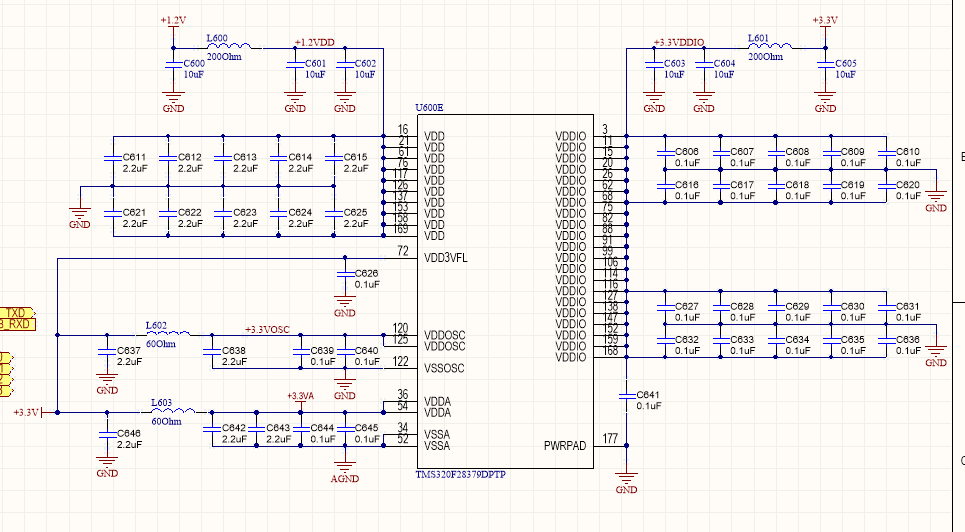
We have designed a custom circuit board that uses the Delfino TMS320F28379D dual core Microcontroller.   For expediency, our original Alpha prototypes used TI’s control card (as a plug in module) which uses the ZWT (ball grid package).  Our Pre-Beta design now uses the PTP (quad flat pack version).   To date, we have built nine of these Pre-Beta units of which (3) would not program CPU2’s FLASH until we slowed the clock down to less than 25MHz.   The 6 other cards would reliably flash both CPU’s at 190MHz.   We have been using an XDS200 USB programmer and Code Composer Version 6.1.1.00022


Here are some additional details:

  1. We initially program CPU1’s and CPU2’s flash with a custom boot loader program using flash algorithms in TI’s F021_API_F2837xD_FPU32.lib that subsequently gets application code from an onboard OMAP processor via a UART.   This bootloader was developed and tested on our Alpha design which utilized TI’s control card and worked without issue.
  2. This initial bootloader program is flashed onto the parts via the JTAG port.  
  3. Using our nine Pre-Beta cards (using the 28379D PTP Package),
    • Code composer’s JTAG test routine works without issue, verifying the JTAG connection for all nine cards
    • 100% of all cards had CPU1 reliably flashed at full rate (190MHz).   Never any issue with CPU1.
    • For six of the cards, CPU2 also programmed at full clock rate.
    • But, three of the cards refused to program until the clock rate was slowed down to 25MHz (using 10MHz internal oscillator and PLL settings of IMULT=15, FMULT=0, IDIV=3 (/6))

FYI:  The Delfino has its boot pins setup for GET MODE.   We have also tried WAIT MODE.  No difference.

The errors indicated (for the three failing cards) from code composer were of two different varieties:

-       The device flash maybe locked, or

-       A break point was unable to be removed at some address.


After much hardware debug and many attempts to get the devices to work (whether changing boot mode, attempts at unlocking flash that was really not locked, etc), we slowed the clock down via code composer properties dialog for PLL settings.   With the integer multiplier set to 15 (multiply by 15) and integer divisor set to 3 (a divide by 6), the remaining three boards flashed.   Ie:   No error messages, no locked flash, no problems with break point removal, just a clean flash load.

Also of note, once any of our delfino’s CPU’s were flashed, they all reliably can be upgraded (re-flashed) via the UART with our bootloader as well as reliably via JTAG at over 100MHz.   Over and Over, no further issues.

We are concerned about moving onto beta and/or production without understanding this issue.   If this is a known problem that slowing the clock down fixes:  OK.  If not known or understood, then we are concerned about experiencing this again at larger volumes.   Also, why did the control card work without issue?   Do they get tested at the factory (ie flashed) so that maybe we would not experience what appears to be an initial programming issue?   Or is there enough of a difference in the boot rom between the two different packages??

Thanks in advance for your help.

  • Michael,

    Thank you for contacting us about your issue.

    Here are a few debug tips to consider:

    1) You mentioned you are using CCSv6.1.1.00022. Could you try checking for updates in CCS and install if any? Especially for TI C2000 Device support package and Debug server Flash package.

    2) When it failed, do you notice any toggle on the XRSn pin?

    3) When it failed, can you check if there is any dip in the voltage lines? Wondering whether supply is able to meet the demand for erase/program operations.

    4) What is CPU1 doing when CPU2 failed? Is it connected and halted? If not, please try that?

    5) Please always use wait boot when programming a fresh device (I see you mentioned other mode as well).

    6) Do you know that all the F2837xD users are suggested to move to CCSv7.4 or greater?
    Please check this FAQ post: e2e.ti.com/.../729543

    7) I would like to bring another thing to your notice. This should not be an issue with CCS, but for your custom loader. You may already know this. But just in case. Please search for "Why is a NMI (due to double bit errors) occurring when Fapi_setActiveFlashBank() is called on F2837xD CPU2?" in the Flash API wiki at processors.wiki.ti.com/.../C2000_Flash_FAQ

    Thanks and regards,
    Vamsi
  • Vamsi,

    Thank you for the quick response!

    A few answers:

    1. Yes, I should have mentioned we installed upgrades for both the C2000 device support and the Debug server flash packages.   We also installed  the emulator update package (I forget its particular name).   I believe it was one of these upgrades that took us from just seeing "your device is locked" to something akin to "break point cannot be removed at...".  

     2 & 3. As you suggested, I will check on the XRS pin state as well as monitor the 3.3V and 1.2V rails.  FYI:  I did use the control card as a reference design for our HW.  The design has supply planes (or heavy polys) for every rail and every major circuit (Osc, analog, core, gnd) and there is a bypass cap at every supply rail as well as filters between those various internal circuits (OSC, analog, core, I/O) as there is on the control card.   Nevertheless, your suggestion makes sense and I'll check our the reset and rails during cpu programming.

    4. CPU1 is halted when we move to program CPU2.   Of course, CCS takes over CPU1 in order to perform this programming.  

    5. In regard to "wait mode"...unfortunately none of our devices are fresh anymore.   But, I understand.   Regardless, using wait mode did not help or change any of the feedback form CCS.

    6. We will upgrade one of our debug platforms to CCS 7.4 as you suggest.  We're a bit stretched right now, so this will be a little lower priority than checking out the rails.   Unless you have some info that says you've seen this issue before and it is fixed with 7.4?

    7.  Thank you for the note about NMI and CPU2.   I forwarded that to our FW team.   In regard to our particular issue....our boot loader works flawlessly at this point.  The problem is constrained to flashing CPU2 when using an emulator.   The problem occurs using CCS and occurs with UniFlash as well.

    Other then a starved supply rail (which I will look at), this smells an awful lot like a race condition in the mailbox logic between cpu1 and cpu2 (solved with a slow clock).   Which may be related to some version of CCS and Uniflash (I have no idea)....but I would suspect therefore that TI would have seen this before?   Are there any known issues along those lines?

    Thanks again for the support..., much appreciated.

    Mike

  • Vamsi,

    FYI: I retested one of the cards looking at the reset and rails as you suggested. When flashing CPU2 at full speed (190MHz) 1.2V droops by 5% and reset goes active. So you were on the money to look there, thank you.

    I will do some further debug in the morning as well as look into the specs on the core during flashing vs our LDO....

    What does the 28379D require for VDD (1.2V) during flashing?

    Thanks again,

    Mike
  • Mike,

    Thank you for answering the questions.

    #1: Could you tell the version of the packages that you are using after the update?

    #2/#3: Ok, please let us know your findings.

    #6: I did not see an issue where slowing down the clock fixed it. But, I would suggest to try 7.4 as your second priority. Please let me know how this goes.

    Can you share the exact error messages? Please enable verbose output mode at the bottom of the On-Chip Flash Plugin GUI - this gives a little more detail.

    Also, generating debug server logs might help for further debug. You can generate the logs via "CCS Help menu -> CCS Support -> Select Debug Server Log -> Click on Properties -> Select Enable Debug Server Logging + Choose a log file location -> Click Ok". Please generate and share them.

    Please note that a few PTP users forgot to solder the PowerPAD on the bottom of the package to the ground plane of the PCB. Debug for this issue started like a Flash debug and later I figured that the user did not solder the powerpad to the ground plane. In another case, 1.2V powersupply line dipped low during the Flash program operation causing a failure. Once they fixed the supply, everything worked fine.

    Thanks and regards,
    Vamsi
  • Vamsi,

    To your (good) question about the PTP package: 

    • Yes, the power pad should be adequately soldered.   I designed the PCB's thermal pad and solder mask per the SLMA002G application note.  
    • I started with TI's footprint (from your website) and only slightly modified it for our needs.   The exposed (solder) pad and paste size is unchanged from TI's recommended footprint.   The only change made was to the number of vias of the larger thermal ground pad (under the device) which are now QTY(200) 10-mil vias. 
    • Our CM typically xrays these and I have pretty good confidence the power pad is both well grounded and has low thermal resistance.

    But, my critical nature says I'm never sure till I am sure :-)   But I believe from a design perspective we're good n that end.

    That said, I think the issue is on the supply side rather than the return.  I have measured VDD (the 1.2V core) dipping 5% (to ~1.4V) just before code composer indicates erasure of CPU2.   I see no 1.2V regulation issues in running operational code, nor any issues (on the 1.2V rail) during erasure/programming of CPU1.   Nor do I see any 3.3V regulation issues.

    At the 5% (dip) point, the supervisor chip resets the delfino which is (clearly) the first layer of the onion as to why programming fails!

    So, this morning I verified all of this again and took the supervisor chip out of the circuit.   In this state, the dip in VDD still occurs, but the erasure and programming of CPU2 successfully completes at 190MHz (because there is no longer a reset).   BTW:  The dip is still the same depth without the reset.

    Clearly this issue is with the 1.2V rail.  It is good to have isolated the issue.  The question is where is the weakness in our design?  

    I will continue to look at the implementation and further bench tests.....BUT, Going back to the spec for a moment: 

    • At design, I referred to Table 5-1 (Device current consumption at 200MHz SYSCLK).  
    • If I had interpreted this correctly, it  indicates during Flash/Erase/Program a max of ~435mA on the 1.2V rail (the sum across the last row).   In operation (the first row), ~500mA.  
    • Therefore I had spec'd and designed in a 1A supply (~2X margin) with (what I thought was) good distribution via planes, adequate vias, and bulk capacitance.

    At this point I wonder if I missed that I should have added the two rows (operation and flashing) and therefore am running marginal???   I would greatly appreciate TI's perspective on the VDD current requirements when JTAG programming CPU2 (which is not in the table) as it requires CPU1 to be running as well.

    One other observation (I don't know if this would be helpful or not), but code composer has three distinct pop-ups during programming of CPU2:

    • First:  Loading CPU1 (with we think is code providing access to CPU2)
    • Second:   Erasing CPU2
    • Third:  Flashing/Programming CPU2.

    The dip in VDD occurs at the end of the first item....(or maybe the beginning of erasing who knows about gui delays).   It is NOT spread over the erasure and there is no dip during programming.   It dips at the transition from downloading a program for CPU1 to the start of erasure of CPU2.

    Anyway, I greatly appreciate your support and thoughts on this problem!

    Mike

  • Mike,

    Looks like I replied before reading your latest reply (I might have started replying while you posted your reply).
    Glad that it helped to check that 1.2V is dipping to 1.14V causing reset in this case.
    I will forward your power questions to our corresponding experts. They can help you further.

    Thanks and regards,
    Vamsi
  • Vamsi,

    I should add some detail from some additional testing today:

    • The "glitch" (causing the reset from the supervisor) at the transition to erasure of CPU2's flash is preceded by a ramp-up in VDD.  See the attached StartOfErasure_IMG1 and IMG2 files at the bottom of this msg.
    • Seeing the ramp, I looked for other similar anomalies and found that at the end of programming I also see a ramp-up of VDD.   See attached EndOfProgramming_IMG3 at the bottom as well.
    • BTW:  All of the above seems to only occur with CPU2 programming.

    So, it seems that somehow the emulator entering and leaving a state of programming of CPU2 influences our regulation of VDD.   I also looked at TI's control card and found that it too displayed glitches at these points in the programming process....BUT VERY SMALL.  

    Adding  (low ESR ceramic) bulk capacitance to our design had little effect as we already have a decent amount.   We're thinking this is now all related to our choice to use an LDO for the 1.2V core rather than a fast switcher as TI has in its control card.

    • As I explained earlier, we used TI's control card as a reference design for our pcb.   We clearly deviated where it made sense to us but tried to stay within the parameters defined by the data sheet.   One area of deviation was VDD.   We have a lot of circuits using 3.3V.   So we have a single switcher for 3.3V for the entire board and chose to use a dedicated LDO for the Delfino's 1.2V VDD.
      • The LDO can only source current whereas it looks like TI's switcher can both source and sink?
      • The LDO is much slower than the 2.5MHz TI switcher
    • What is the source of the energy for the ramp-up in VDD?   Since the LDO cannot sink current, it will shut off its supply as VDD rises above its target voltage.  It's load regulation is typically  better than 0.5%.  When a load then occurs it will be relatively slow to react and hence the glitch down(?)
    • Can the Delfino under certain conditions backfeed current out of VDD???

    We plan on a spin before Beta (soon) and need to understand the changes in this area.   We do not want to add another switcher as we have invested a lot of effort in getting fidelity out of our analog circuits and minimizing sampling noise.   So keeping things quiet is paramount.   Can TI recommend an LDO for use here?

    In general, I am wondering what we missed in the data sheet and design guides for the BW of the VDD supply?   I have also attached a screen shot of our PCB's Delfino's bypass caps and supply filtering.   I believe(?) this duplicates the control cards design from this perspective.   Of course there is bulk not shown (140uF+ on VDD for example).  These are at the pins with vias straight to planes.

    Anyway, I appreciate your and your team's support and suggestions!!!  I think we have a handle on the root cause of the flashing clock rate issue (reset due to VDD glitch) and now need to understand the design change required to fix it.

    Thanks again,

    Mike

  • Mike,

    You have done a really good job working through this issue and communicating the observations, it presents a clear picture of what is going on.  Let me summarize the sequence as I understand it and some steps to avoid the issue.

    1)      When programming CPU2, the GEL file might be putting the device into a lower power condition.

    1. Once entering low power state the VDD rises, as described in this advisory:
          Low-Power Modes: Power Down Flash or Maintain Minimum Device Activity
          http://www.ti.com/product/TMS320F28379D/technicaldocuments#doctype3
    2. TI will look at what is going on here as this is unexpected to me, but that will be longer term than what you need.
    3. To mitigate this and avoid the VDD rise, you could increase the VDD current consumed by the device before initiating flash programming. Enabling some peripheral clocks via the PCLKCRx registers with a CCS script can probably increase the device current sufficiently.
    4. Adding a DC load (100-200 ohm resistor between VDD and VSS) could also avoid this rise, but obviously may not be desirable for the extra static current.

    2)      System 1.2v LDO shuts off due to VDD rise [speculative but reasonable]

    1. With a VDD rise, the LDO may be fully ‘off’. This could make it susceptible to not respond well to step-increase in current demand, whereas it might have been okay if still operating in active region

    3)      Flash tools are enabling PLL at user specified frequency

    1. Transition from low to high frequency causes a large step-increase in current demand

                                                        i.     Droops VDD to -5% due to slow LDO

                                                       ii.     Supervisor trips

                                                      iii.     Interrupts Erase

    1. Programming Flash with a lower frequency solves this issue since the current step increase is smaller and the LDO has more time to respond.
    2. A faster LDO could also fix this, unfortunately I’m not an expert in this selection.
    3. When adding the low-ESR bulk cap, was it directly on the LDO output or on the F28379D side of the ferrite? I’m not sure about LDO design requirements, but putting cap on the device side of the ferrite could help given the fast change in current.

    Note that if the application has any step-increase in current during normal operation then the same thing could occur.  I think you are correct that a faster LDO or re-design of the VDD filter is needed.

    Best regards,

    Jason

  • Jason,

    Thank you for your response.

    The link you sent refers back to the Errata: advisory on the 3,3V Flash supply leakage onto the 1.2VDD ....which nails this problem on the head:   The ramp up is quite linear and the LDO shut off guaranteed.  Thank you for pointing this out.

    I already had a 1.2K shunt on the LDO per the manufacturer's requirement for min current consumption.   So, per your suggestion, I changed that (as a test) this morning to 100 ohms and all 7 boards I modified worked, rise and downward glitch gone,   The supervisor chip is happy and so am I.

    I believe in our application we should have enough runtime consumption to avoid this phenomenon outside of the JTAG programming.   However, I'm never happy ignoring something.   Also, I don't think a faster LDO is the answer as the rise itself is a problem if it is uncontrolled.   The current LDO we're using has a built in sink that triggers at 6.5% above...which is not good enough for the delfino's requirement of +/-5%

    Also, We'd like to avoid a switcher.  I think the control card doesn't see this as it is a two fet (source and sink) switcher.    Can TI point to an LDO or non-switcher implementation for the delfino considering this leakage path exists?

    If not, the 100-ohm maybe a viable answer (we are a hard wired product).... if you can provide a spec on the max leakage current???

    On a related subject (1.2VDD and reset):   In terms of power supply sequencing, is there really any requirement that the 1.2V rise within 10mS of the 3.3V supplies?   The spec seems to imply that only real concern is A) that all of the 3.3V inputs come up at the same time and B) that the 3.3V are a higher potential than the 1.2V VDD.

    I ask this as we got concerned about sequencing when considering the issues at shutdown:  That is, ensuring 1.2V is always below 3.3V (as it bleeds down differently due to different capacitive loading).   So we built in a FET controlled sink based upon the 3.3V supervisor's undervoltage detector.   This works well for the shutdown, but has the effect that the 1.2V will not come up until the 3.3V is stable.  

    I think we can ultimately achieve the 10ms, but right now we are at 20mS.   FYI:  Reset is held active until both supplies are fully stable at the right voltages.

    Does this make sense?

    Thanks again for the support.

    Mike

  • Mike,

    Glad we’ve converged. FYI, I may edit my posts for clarity later in case others reference it.

    Getting into the details, each Flash Bank can provide up to 6.4mA of current from VDD3VFL to VDD. When you began programming the second bank, this woke up the second bank and resulted in about 12.8mA of total current. This explains why programming CPU1’s bank never had a problem as well, the natural device VDD leakage was sufficient to consume the first 6.4mA.

    For a resistor value, assuming a 10% resistor tolerance to consume the worst case 12.8mA current it looks like you will need an 82 Ohm resistor between VDD and VSS. This is a little overkill since it does not include any of the normal beneficial device VDD leakage, but will cover all cases across low temperature when VDD leakage is small as well.

    I agree with you on the general LDO speed, that is not the solution since the LDO is getting completely out of its regulation range. What is needed is an LDO which has inbuilt push-pull current sink capability. I could not find one of these on an initial search, I'm going to keep looking though.


    To your second line of questions on VDD and VDDIO supply sequencing, in looking for LDOs I did find one (there are others) with an under-voltage lockout feature to help with VDDIO and VDD sequencing within 1-2ms. You might see if this meets your needs, let me know any feedback.
    www.ti.com/.../TLV757P
    If you add the 82 Ohm resistor, then this portion of concern may be moot since that should pull the supply low quickly on shutdown.


    I also want to let you know, we do have a pending Advisory on supply sequencing. If VDDOSC is on while VDD is off in a static condition, then there will be downward frequency drift on the INTOSC1 and INTOSC2 circuits that will accumulate. Your set up sounds okay, but minimizing the time of the supplies on without the other should be done. Our recommendation is to power all supplies together. It is worth noting that this particular upcoming Advisory is not a concern for most applications which use a crystal on X1/X2 as the primary clock source since the XTAL circuit is separate and not at all impacted.

    Best regards,
    Jason
  • Jason,

    Convergence is good ....Its nice to have a smoking gun! Thank you for the design details and added information.

    Thanks for the link to the TLV757P. Currently, the part I'm using has an enable that is tied to the 3.3V supervisor's under voltage. But your part's active (built in) discharge maybe adequate and save external parts.. I'll look at more closely, thank you.

    If it is possible for me to receive and alert on the upcoming advisory I would appreciate it.

    Thanks again for the support.

    Mike
  • Mike,

    I don't know if you've used one of our part selection tools, in case a different LDO might have different features you'd like.  This is how I found the TLV757P

    http://www.ti.com/power-management/linear-regulators-ldo/products.html#p451max=1;1.5&p238max=3.3;12&p238min=0;3.3&p634max=1.2;125&p634min=-37;1.2&p1155=0.75;1 

    If you click on the right side 'Alert Me' button you will receive updates for everything in this product folder.

    Thanks for your patience.  I know this debug wasn't planned as I'm sure you have other things to do as you finalize your product.  I hope all goes well with everything else!

    Best regards,

    Jason

  • Always plenty to do. Thanks again Jason.

    -Mike