This thread has been locked.

If you have a related question, please click the "Ask a related question" button in the top right corner. The newly created question will be automatically linked to this question.

TMS32028379D DMA Priority

Good afternoon, TI.

Tell me please what will happen in the next situation, maybe you can tell me how best to do it.
I am using TMS32028379D.
I have a synchronous measurement of ADC 1 (A) and ADC 2 (B), while each ADC has its own DMA channel (1 ( high priority) and 2) and configured the ripping vector ADCINTA1, ADCINTB1 for each SOC of the ADC.
I also use the DMA channel 4,5,6 (configured).

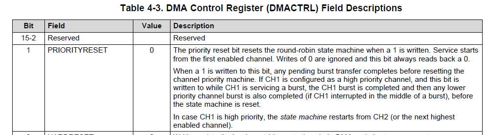
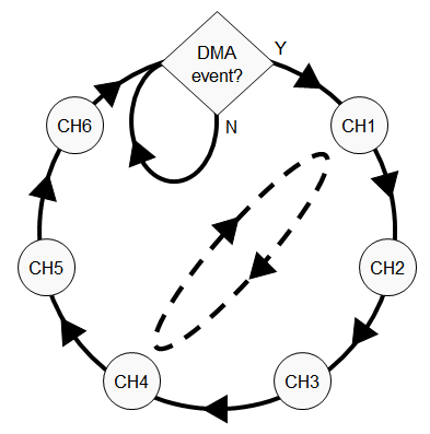
In the case when I am processing the DMA 4 channel, the ADCINTA1 and ADCINTB1 interrupt is triggered at the same time, the data is unloaded from the DMA 1 priority channel, after the DMA1 download is completed, the DMA2 will go to the processing, or return to channel 4, 5.6 and only after Processing them to channel 2? Channel 2 is configured to interrupt ADCINTB1 which is triggered simultaneously with ADCINTA1.

My task is to make it so that when the ADCINTA1 and ADCINTB1 snagging is triggered, the information from ADCs A and B is unloaded into RAM with priority No. 1 by means of DMA CH1 and DMA CH2. Perhaps you can tell me how to set up DMA 1 so that it processes ADC A and ADC B in turn. Or how can I set high Prioryty on CH1 and CH2.

  • Hi Serhii Chekanov,

    Have you read Section 4.5 "Channel Priority" within the Technical Reference Manual for this device?

    http://www.ti.com/lit/spruhm8

    Neither the 'Round-Robin' or 'Channel 1 High Priority' modes meet the application you described, if more than CH1 and CH2 are enabled.

    The PRIORITYRESET bit of the DMACTRL register could possibly be useful, however "any pending burst transfer completes before resetting the channel priority machine". i.e. it may only be useful if there are no pending transfers while CH1 is being serviced.

    The F28379D having two CPUs each with their own respective DMA, maybe there's a way you could use one for ADC A and the other for B.

    Hope this helps,

    Kevin

  • Hi Kevin! Yes, i already read that information in reference manual, and i cant use second core becouse in the end i will work with tms32028075. Can you help me recive results from adca and adcb in correct seqyence DMA chenal1 and chenal2
  • Hi Serhii Chekanov,

    Your ADC samples are occurring fast enough to where the DMA state machine can't make its way back to CH1 or CH2 in time? What you are using DMA channels 4, 5, & 6 for? Can you further explain how your ADC sampling is occurring?

    i.e. What is triggering the SOC for ADC A & B sampling? what is the sampling frequency for each?

    Best,

    Kevin

  • Hi Kevin!

    My settings ADC and DMA 1,2/

    EALLOW;

    PieCtrlRegs.PIEIER1.bit.INTx1 = 0; // Enable ADCAINT in PIE group 1
    PieCtrlRegs.PIEIER1.bit.INTx2 = 0; // Enable ADCBINT in PIE group 1

    DmaRegs.CH1.CONTROL.bit.HALT = 1; // ДМА от АДЦ А
    DmaRegs.CH2.CONTROL.bit.HALT = 1; // ДМА от АДЦ Б

    CpuSysRegs.PCLKCR13.bit.ADC_A = 1;
    CpuSysRegs.PCLKCR13.bit.ADC_B = 1;
    // CpuSysRegs.PCLKCR13.bit.ADC_D = 1;
    //ADC_cal();

    AdcaRegs.ADCCTL2.bit.PRESCALE = 3; //set ADCCLK divider to /2,5 , 120/ 2.5 = 48 MHz
    AdcbRegs.ADCCTL2.bit.PRESCALE = 3; //set ADCCLK divider to /2,5 , 120 /2.5 = 48 MHz

    AdcSetMode(ADC_ADCA, ADC_RESOLUTION_12BIT, ADC_SIGNALMODE_SINGLE);
    AdcSetMode(ADC_ADCB, ADC_RESOLUTION_12BIT, ADC_SIGNALMODE_SINGLE);

    //
    //Set pulse positions to late
    //
    AdcaRegs.ADCCTL1.bit.INTPULSEPOS = 1;
    AdcbRegs.ADCCTL1.bit.INTPULSEPOS = 1;

    EDIS;


    EALLOW;
    AdcaRegs.ADCCTL1.bit.ADCPWDNZ = 1; // Power up ADCA
    DELAY_US(1000);

    AdcbRegs.ADCCTL1.bit.ADCPWDNZ = 1; // Power UP ADCB
    DELAY_US(1000); //

    EDIS;

    EALLOW;

    AdcaRegs.ADCSOC0CTL.bit.CHSEL = ADCIN3;
    AdcaRegs.ADCSOC1CTL.bit.CHSEL = ADCIN4;
    AdcbRegs.ADCSOC0CTL.bit.CHSEL = ADCIN15;
    AdcbRegs.ADCSOC1CTL.bit.CHSEL = ADCIN3;

    AdcaRegs.ADCSOC2CTL.bit.CHSEL = ADCIN0;
    AdcaRegs.ADCSOC3CTL.bit.CHSEL = ADCIN1;
    AdcaRegs.ADCSOC4CTL.bit.CHSEL = ADCIN5;

    AdcbRegs.ADCSOC2CTL.bit.CHSEL = ADCIN2;
    AdcbRegs.ADCSOC3CTL.bit.CHSEL = ADCIN4;
    AdcbRegs.ADCSOC4CTL.bit.CHSEL = ADCIN1;
    EDIS;

    EALLOW;

    AdcaRegs.ADCSOC0CTL.bit.ACQPS = 12; // SOC S/H Window (1/120 000 000)* 12+1 = 108
    AdcaRegs.ADCSOC1CTL.bit.ACQPS = 12; //
    AdcbRegs.ADCSOC0CTL.bit.ACQPS = 12; //
    AdcbRegs.ADCSOC1CTL.bit.ACQPS = 12; //

    AdcaRegs.ADCSOC2CTL.bit.ACQPS = 12; //
    AdcaRegs.ADCSOC3CTL.bit.ACQPS = 12; //
    AdcaRegs.ADCSOC4CTL.bit.ACQPS = 12; //

    AdcbRegs.ADCSOC2CTL.bit.ACQPS = 12; //
    AdcbRegs.ADCSOC3CTL.bit.ACQPS = 12; //
    AdcbRegs.ADCSOC4CTL.bit.ACQPS = 12; //
    EDIS;


    //*********************************************************************************************
    //
    // ADCTRIG9 - EPWMA2 10 mks, ADCTRIG15 - EPWM6A - 30mks
    //*********************************************************************************************

    EALLOW;

    AdcaRegs.ADCSOC0CTL.bit.TRIGSEL = ADCTRIG7; // SOC S/H Window (1/120 000 000)* 12+1 = 108
    AdcaRegs.ADCSOC1CTL.bit.TRIGSEL = ADCTRIG7; //
    AdcbRegs.ADCSOC0CTL.bit.TRIGSEL = ADCTRIG7; //
    AdcbRegs.ADCSOC1CTL.bit.TRIGSEL = ADCTRIG7; // ADC trigger

    AdcaRegs.ADCSOC2CTL.bit.TRIGSEL = ADCTRIG15; //
    AdcaRegs.ADCSOC3CTL.bit.TRIGSEL = ADCTRIG15; //
    AdcaRegs.ADCSOC4CTL.bit.TRIGSEL = ADCTRIG15; //

    AdcbRegs.ADCSOC2CTL.bit.TRIGSEL = ADCTRIG15; //
    AdcbRegs.ADCSOC3CTL.bit.TRIGSEL = ADCTRIG15; //
    AdcbRegs.ADCSOC4CTL.bit.TRIGSEL = ADCTRIG15; //
    EDIS;

    EALLOW;

    AdcaRegs.ADCSOCPRICTL.bit.SOCPRIORITY = 2; // SOC0, SOC1 Higest priority , 00 No priority, 01 - priority SOC0 etc.
    AdcaRegs.ADCSOCPRICTL.bit.SOCPRIORITY = 2; // SOC0, SOC1 Higest priority

    EDIS;

    EALLOW;

    AdcbRegs.ADCSOCPRICTL.bit.SOCPRIORITY = 2; // SOC0, SOC1 Higest priority , 00 No priority, 01 - priority SOC0 etc.
    AdcbRegs.ADCSOCPRICTL.bit.SOCPRIORITY = 2; // SOC0, SOC1 Higest priority

    EDIS;


    EALLOW;

    AdcaRegs.ADCINTSEL1N2.bit.INT1SEL = 0; //end of SOC0 will set INT1А flag
    AdcaRegs.ADCINTSEL1N2.bit.INT1E = 1; //enable INT1А flag
    AdcaRegs.ADCINTFLGCLR.bit.ADCINT1 = 1; //make sure INT1А flag is cleared

    EDIS;

    EALLOW;

    AdcbRegs.ADCINTSEL1N2.bit.INT1SEL = 0; //end of SOC0 will set INT1Б flag
    AdcbRegs.ADCINTSEL1N2.bit.INT1E = 1; //enable INT1Б flag
    AdcbRegs.ADCINTFLGCLR.bit.ADCINT1 = 1; //make sure INT1Б flag is cleared

    EDIS;


    DMACH1Config();
    DMACH2Config();

    EALLOW; // This is needed to write to EALLOW protected registers
    PieVectTable.ADCA1_INT = &HWI_ADC;
    PieVectTable.ADCB1_INT = &HWI_ADC;
    EDIS; // This is needed to disable write to EALLOW protected registers

    PieCtrlRegs.PIEIER1.bit.INTx1 = 1; // Enable ADCAINT in PIE group 1
    PieCtrlRegs.PIEIER1.bit.INTx2 = 1; // Enable ADCBINT in PIE group 1
    IER |= M_INT1; // Enable INT1 in IER to enable PIE group

    }

    Settings DMA1, DMA2 have same settings.

    EALLOW;
    // Reset selected channel via CONTROL Register:
    DmaRegs.CH1.CONTROL.bit.SOFTRESET = 1; // Perform SOFT reset on channel (clears all counters)

    DmaRegs.PRIORITYCTRL1.bit.CH1PRIORITY = 1; // Set Channel 1 DMA to highest priority

    // Set up MODE Register:
    DmaRegs.CH1.MODE.bit.PERINTSEL = DMA_ADCBINT1;// DMA_ADCBINT1
    DmaRegs.CH1.MODE.bit.PERINTE = 1; // Peripheral interrupt enabled
    DmaRegs.CH1.MODE.bit.ONESHOT = 0; // 1 burst per SW interrupt
    DmaRegs.CH1.MODE.bit.CONTINUOUS = 1; //
    // DmaRegs.CH1.MODE.bit.SYNCE = 0; //
    // DmaRegs.CH1.MODE.bit.SYNCSEL = 0; //
    DmaRegs.CH1.MODE.bit.DATASIZE = 0; //
    DmaRegs.CH1.MODE.bit.CHINTMODE = 1; //
    DmaRegs.CH1.MODE.bit.CHINTE = 0; //


    // Set up BURST registers:

    DmaRegs.CH1.BURST_SIZE.all = 4;

    DmaRegs.CH1.SRC_BURST_STEP = 0x0001; //
    DmaRegs.CH1.DST_BURST_STEP = 0x0001; //

    // Set up TRANSFER registers:
    DmaRegs.CH1.TRANSFER_SIZE = 0; // =1 Bursts (N-1) per transfer
    DmaRegs.CH1.SRC_TRANSFER_STEP = 0; //
    DmaRegs.CH1.DST_TRANSFER_STEP = 0; //

    // Set up WRAP registers:
    DmaRegs.CH1.SRC_WRAP_SIZE = 0xFFFF; //
    DmaRegs.CH1.DST_WRAP_SIZE = 0xFFFF; //
    DmaRegs.CH1.SRC_WRAP_STEP = 0;
    DmaRegs.CH1.DST_WRAP_STEP = 0;

    // Set up SOURCE address:
    DmaRegs.CH1.SRC_BEG_ADDR_SHADOW = (Uint32)&AdcaResultRegs.ADCRESULT0; //
    DmaRegs.CH1.SRC_ADDR_SHADOW = (Uint32)&AdcaResultRegs.ADCRESULT0; //

    // Set up DESTINATION address:
    DmaRegs.CH1.DST_BEG_ADDR_SHADOW = (Uint32)&measMem.Iu_adc; //
    DmaRegs.CH1.DST_ADDR_SHADOW = (Uint32)&measMem.Iu_adc; //

    // Clear any spurious flags:
    DmaRegs.CH1.CONTROL.bit.PERINTCLR = 1; // Clear any spurious interrupt flags
    // DmaRegs.CH1.CONTROL.bit.SYNCCLR = 1; // Clear any spurious sync flags
    DmaRegs.CH1.CONTROL.bit.ERRCLR = 1; // Clear any spurious sync error flags

    DmaRegs.CH1.MODE.bit.OVRINTE = 0; // Enable/disable the overflow interrupt
    DmaRegs.CH1.CONTROL.bit.RUN = 1;

    EDIS;

  • I use DMA CH4,5 For semaphore (10ms , 30 cycle). CH6 Reserv.

    Information about my settings is checking by moderator, and i think it will appear soon.


  • I need something like that.

  • Hi Serhii Chekanov,

    You're wanting CH1, CH2, and CH4 to have equal priority and higher than all the other channels then? I don't see this being possible if you have more than just these three channels enabled. Only CH1 is able to have a higher priority.

    Within your application is the DMA state machine not able to work its way around to service CH1,2, & 4 in time when using round-robin mode?

    Best,
    Kevin
  • Hi, Kevin!

    Thanks for ansver, could you help me to calculate time for service every chenal. May be you have manual or recomendations.

  • Hi Serhii Chekanov,

    Please take a look at section 4.3, "Pipeline Timing and Throughput", of the F28379D Manual. It should assist you with calculating the service time based on your configuration.

    http://www.ti.com/lit/spruhm8

    Best,

    Kevin