


Other Parts Discussed in Thread: AMC1303E2510, AMC1306M25
Hi,
I'm using Filters1, 2 and 3 of the TMS320F28075 SDFM1 to read the Manchester Encoded output from 3 separate AMC1303E2510 chips. The AMC1303E2510 has it's own internally generated 10MHz CLK, therefore I'm using CMPC and CMPD of ePWM11 to synchronise filters1, 2 and 3 of SDFM1. After the result from each Filter is read, it is re-scaled to the DAC range (0-4095) and the 3 filter outputs are output on the 3 DACs. I've attached the main .c file of the project below.
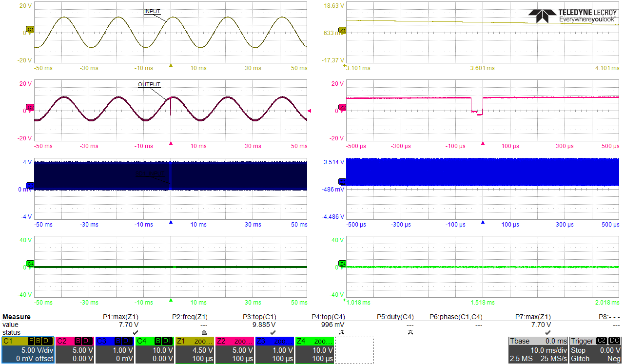
The problem I have is that the output from the SDFM module is wrong sometimes. In the oscilloscope shot below:
- CH1 (yellow) is a +/-10V input (via resistor divider) to the AMC1303 chip for Filter 1. +/-10V produces +/-250mV at the AMC1303 input.
- CH2 (pink) is the DAC output for Filter 1 (note that it is passed through an external op-amp buffer to increase it's amplitude).
You can see in the zoom in of CH2 that the DAC output is wrong for approx. 40us (in the code the SDFM sampling period is approx. 20us so this corresponds to 2 incorrect values from the SDFM module). I have also verified that the problem is not with the conversion to the DAC (i.e. the raw data read from the SDDATA register for filter 1 is incorrect).
The ISR routine, epwm1_isr, is triggered when ePWM1 counter is 0. It is configured in UP COUNT mode. The PWM period is set to 4 times the SDFM sampling period. This is because after a PWM sync, the first two SDFM output values are incorrect (with a SINC3 filter). ePWM11 is setup the same as ePWM1 and is synced to the ePWM1 counter by the synchronisation pulse input from ePWM1 fed through ePWM10.
ePWM11.CMPC and CMPD are set to SDFM_RESET_CMP_VALUE. SDFM_RESET_CMP_VALUE is set so that it occurs Latency of data filter + 5 SD clock cycles before the PWM counter resets to 0. Therefore after the CMPC/CMPD PWM sync there should be time for 3 SDFM output values before the ISR triggers. Therefore I'm confident that the problem is not because I am reading one of the 2 incorrect samples after a PWMSYNC event.
In the ISR the ACK and the Modulator failure flags for filters 1, 2 and 3 are checked. If any of the ACK flags are NOT set or if any of the modulator failure flags are set, then the routine pauses (using ESTOP0). However this never happens, even when there is an incorrect value.
Finally, I have seen in the datasheet and other threads that the delta-sigma chip (AMC1303E2510 in this case) CLK period must be between 8*T_SYSCLK - 20*T_SYSCLK. In my code I am using the line
InitSysPll(INT_OSC2,IMULT_10,FMULT_0,PLLCLK_BY_1);
to set the MCU CLK frequency to 100MHz. Therefore T_SYSCLK = 10ns. So the delta-sigma CLK period must be between 80ns - 200ns. For a 10MHz delta-sigma CLK, the period is 100ns so that should be fine.
Do you see anything wrong with the setup I have described? Have you seen this kind of behaviour before?
Many thanks,
Fearghal
//###########################################################################
//
// FILE:   sdfm_pwm_sync_cpu_cpu01.c
//
// TITLE:  SDFM PWM sync Example for F2807x.
//
//! \addtogroup cpu01_example_list
//! <h1> SDFM PWM Sync </h1>
//!
//! In this example, SDFM filter data is read by CPU in SDFM ISR routine. The
//! SDFM configuration is shown below:
//!     - SDFM1 is used in this example
//!     - MODE2 Input control mode selected
//!     - Comparator settings
//!         - Sinc3 filter selected
//!         - OSR = 32
//!         - HLT = 0x7FFF (Higher threshold setting)
//!         - LLT  = 0x0000(Lower threshold setting)
//!  -  Data filter settings
//!      - 3 filter modules enabled
//!      - Sinc3 filter selected
//!      - OSR = 50
//!      - All the 3 filters are synchronized by using PWMSYNC
//!      - Filter output represented in 16 bit format
//!      - In order to convert 25 bit Data filter
//!        into 16 bit format user needs to right shift by 2 bits for
//!        Sinc3 filter with OSR = 50
//!  - Interrupt module settings for SDFM filter
//!      - All the 4 higher threshold comparator interrupts disabled
//!      - All the 4 lower threshold comparator interrupts disabled
//!      - All the 4 modulator failure interrupts disabled
//!      - All the 4 filters will NOT generate an interrupt when a new filter data
//!        is available
//!      - The interrupt is controlled by ePWM1
//!
//
//###########################################################################
// $TI Release: F2807x Support Library v3.05.00.00 $
// $Release Date: Tue Jun 26 03:19:11 CDT 2018 $
// $Copyright:
// Copyright (C) 2014-2018 Texas Instruments Incorporated - http://www.ti.com/
//
// Redistribution and use in source and binary forms, with or without
// modification, are permitted provided that the following conditions
// are met:
//
//   Redistributions of source code must retain the above copyright
//   notice, this list of conditions and the following disclaimer.
//
//   Redistributions in binary form must reproduce the above copyright
//   notice, this list of conditions and the following disclaimer in the
//   documentation and/or other materials provided with the
//   distribution.
//
//   Neither the name of Texas Instruments Incorporated nor the names of
//   its contributors may be used to endorse or promote products derived
//   from this software without specific prior written permission.
//
// THIS SOFTWARE IS PROVIDED BY THE COPYRIGHT HOLDERS AND CONTRIBUTORS
// "AS IS" AND ANY EXPRESS OR IMPLIED WARRANTIES, INCLUDING, BUT NOT
// LIMITED TO, THE IMPLIED WARRANTIES OF MERCHANTABILITY AND FITNESS FOR
// A PARTICULAR PURPOSE ARE DISCLAIMED. IN NO EVENT SHALL THE COPYRIGHT
// OWNER OR CONTRIBUTORS BE LIABLE FOR ANY DIRECT, INDIRECT, INCIDENTAL,
// SPECIAL, EXEMPLARY, OR CONSEQUENTIAL DAMAGES (INCLUDING, BUT NOT
// LIMITED TO, PROCUREMENT OF SUBSTITUTE GOODS OR SERVICES; LOSS OF USE,
// DATA, OR PROFITS; OR BUSINESS INTERRUPTION) HOWEVER CAUSED AND ON ANY
// THEORY OF LIABILITY, WHETHER IN CONTRACT, STRICT LIABILITY, OR TORT
// (INCLUDING NEGLIGENCE OR OTHERWISE) ARISING IN ANY WAY OUT OF THE USE
// OF THIS SOFTWARE, EVEN IF ADVISED OF THE POSSIBILITY OF SUCH DAMAGE.
// $
//###########################################################################

//
// Included Files
//
#include "F28x_Project.h"
#include "F2807x_struct.h"
#include "F2807x_sdfm_drivers.h"

/* Device Related Defines */
#define CPU_SYS_CLOCK (100*1000000)
#define PWMSYSCLOCK_FREQ (50*1000000)
#define ECAPSYSCLOCK_FREQ   (100*1000000)

//
// User Defines
//
#define SDFM_MODE                   MODE_2
#define SDFM_FILTER_TYPE            SINC3
#define SDFM_OSR                    OSR_50          // Value is for OSR_50 is actually 49
#define SDFM_NUM_BITS_RIGHT_SHIFT   SHIFT_2_BITS    // This setting depends on the OSR and filter type. See datasheet for details
#define SDFM_SCALE_FACTOR           0.00001525878906 // = ( 0.5 / 32768.0 ). This assumes that the SDFM output is from -32768 to 32767 (i.e. int16_t)

#if SDFM_FILTER_TYPE == SINCFAST
#define     NUM_INCORRECT_SAMPLES_AFTER_SYNC    2
#elif SDFM_FILTER_TYPE == SINC1
#define     NUM_INCORRECT_SAMPLES_AFTER_SYNC    0
#elif SDFM_FILTER_TYPE == SINC2
#define     NUM_INCORRECT_SAMPLES_AFTER_SYNC    1
#elif SDFM_FILTER_TYPE == SINC3
#define     NUM_INCORRECT_SAMPLES_AFTER_SYNC    2
#endif

#define SDCLK_FREQ          ( 0.96 * 10000000.0 )        // delta-sigma device dependent if the chip uses it's own internal CLK. Use lowest possible frequency
#define SD_OUTPUT_FREQ      ( SDCLK_FREQ / (float)(SDFM_OSR + 1) )
#define PWM_CLK_IN_SDFM_CLK ( PWMSYSCLOCK_FREQ / SDCLK_FREQ )
#define PWM_CLK_IN_SDFM_OSR ( PWMSYSCLOCK_FREQ / SD_OUTPUT_FREQ )

// Define the filter latencies. Add 5 SD CLK cycles as per datasheet.
// Use 0.96*SDCLK_FREQ to account for 4% tolerance on the internal CLK frequency
// of the AMC1303
#define SDFM2_LATENCY_PWM_CLK_COUNT     ( ( (NUM_INCORRECT_SAMPLES_AFTER_SYNC + 1) * PWM_CLK_IN_SDFM_OSR ) + ( 5.0 * PWM_CLK_IN_SDFM_CLK ) )
#define EPWM_TIMER_PERIOD               ( (NUM_INCORRECT_SAMPLES_AFTER_SYNC + 2) * PWM_CLK_IN_SDFM_OSR )
#define SDFM_RESET_CMP_VALUE            ( EPWM_TIMER_PERIOD - SDFM2_LATENCY_PWM_CLK_COUNT )

//
// SDFM Defines
//
#define SDFM_PIN_MUX_OPTION1      1
#define SDFM_PIN_MUX_OPTION2      2
#define SDFM_PIN_MUX_OPTION3      3

//
// DAC Defines
//
#define REFERENCE_VDAC              0
#define REFERENCE_VREF              1
#define DACA                        1
#define DACB                        2
#define DACC                        3
#define DAC_REFERENCE_VOLTAGE       REFERENCE_VREF

//
// ePWM Defines
//
#define EPWM1_TIMER_TBPRD       EPWM_TIMER_PERIOD  // Period register

#define EPWM10_TIMER_TBPRD      EPWM_TIMER_PERIOD  // Period register

#define EPWM11_TIMER_TBPRD      EPWM_TIMER_PERIOD  // Period register
#define EPWM11_CMPC             SDFM_RESET_CMP_VALUE
#define EPWM11_CMPD             SDFM_RESET_CMP_VALUE

#define EPWM12_TIMER_TBPRD      EPWM_TIMER_PERIOD  // Period register
#define EPWM12_CMPC             SDFM_RESET_CMP_VALUE
#define EPWM12_CMPD             SDFM_RESET_CMP_VALUE

#define EPWM_CMP_UP           1
#define EPWM_CMP_DOWN         0

//
// Globals
//
uint16_t gPeripheralNumber, gPWM_number = 12;
int16_t  Filter1_Result = 0;
int16_t  Filter2_Result = 0;
int16_t  Filter3_Result = 0;
int16_t  Filter4_Result = 0;
uint16_t  SDFMReadingCounter = 0;
uint32_t sdfmReadFlagRegister;

#pragma DATA_SECTION(Filter1_Result,"Filter1_RegsFile");
#pragma DATA_SECTION(Filter2_Result,"Filter2_RegsFile");
#pragma DATA_SECTION(Filter3_Result,"Filter3_RegsFile");
#pragma DATA_SECTION(Filter4_Result,"Filter4_RegsFile");
volatile struct DAC_REGS* DAC_PTR[4] = {0x0,&DacaRegs,&DacbRegs,&DaccRegs};

//
// Function Prototypes
//
void Sdfm_configurePins(uint16_t);
void InitEPwm(void);
void done(void);
void GPIO_configureDiagnosticPins(void);
void GPIO_setOutputValue(uint32_t GPIONumber, uint32_t outputValue);
void GPIO_setOutputValue43(uint32_t GPIONumber, uint32_t outputValue);
void configureDAC(Uint16 dac_num);
__interrupt void Sdfm2_ISR(void);

void InitEPwm1Example(void);
void InitEPwm10Example(void);
void InitEPwm11Example(void);
void InitEPwm12Example(void);
__interrupt void epwm1_isr(void);

// Debug variables
#define MEMORY_SIZE     16
uint32_t SDFM_ISR_counter = 0;
int16_t  Filter2_Result_Memory[MEMORY_SIZE];
int16_t  Filter3_Result_Memory[MEMORY_SIZE];
uint16_t memory_pointer = 0;
int32_t debug_1 = EPWM1_TIMER_TBPRD;
int32_t debug_2 = SDFM_RESET_CMP_VALUE;
uint32_t CH1_ACTIVE;
uint32_t CH2_ACTIVE;
uint32_t CH3_ACTIVE;
uint32_t FAULT;

//
// Main
//
void main(void)
{
   uint16_t  pinMuxoption;
   uint16_t  HLT, LLT;

//
// Initialize System Control:
// PLL, WatchDog, enable Peripheral Clocks
// This example function is found in the F2807x_SysCtrl.c file.
//
    InitSysCtrl();

//
// Clear all __interrupts and initialize PIE vector table:
// Disable CPU __interrupts
//
    DINT;

//
// Initialize PIE control registers to their default state.
// The default state is all PIE __interrupts disabled and flags
// are cleared.
// This function is found in the F2807x_PieCtrl.c file.
//
    InitPieCtrl();

//
// Disable CPU __interrupts and clear all CPU __interrupt flags:
//
    IER = 0x0000;
    IFR = 0x0000;

//
// Initialize the PIE vector table with pointers to the shell Interrupt
// Service Routines (ISR).
// This will populate the entire table, even if the __interrupt
// is not used in this example.  This is useful for debug purposes.
// The shell ISR routines are found in F2807x_SysCtrl.c.
// This function is found in F2807x_SysCtrl.c.
//
    InitPieVectTable();

//
// Interrupts that are used in this example are re-mapped to
// ISR functions found within this file.
//
    EALLOW;
    PieVectTable.EPWM1_INT = &epwm1_isr;
    PieVectTable.SD2_INT = &Sdfm2_ISR;
    EDIS;

    //
    // For this example, only initialize the ePWM
    //
    EALLOW;
    CpuSysRegs.PCLKCR0.bit.TBCLKSYNC = 0;
    EDIS;

    InitEPwm1Example();
    InitEPwm10Example();
    InitEPwm11Example();
    InitEPwm12Example();

    EALLOW;
    CpuSysRegs.PCLKCR0.bit.TBCLKSYNC = 1;
    EDIS;


//
// Configure DACA and DACB
//
    configureDAC(DACA);
    configureDAC(DACB);
    configureDAC(DACC);


#ifdef CPU1
    pinMuxoption = SDFM_PIN_MUX_OPTION1;
//
// Configure GPIO pins as SDFM pins
//
    Sdfm_configurePins(pinMuxoption);
#endif

//
// Select SDFM1
//
    gPeripheralNumber = SDFM1;

//
// Input Control Module
//
// Configure Input Control Mode: Modulator Clock rate = Modulator data rate
//
    Sdfm_configureInputCtrl(gPeripheralNumber, FILTER1, SDFM_MODE);
    Sdfm_configureInputCtrl(gPeripheralNumber, FILTER2, SDFM_MODE);
    Sdfm_configureInputCtrl(gPeripheralNumber, FILTER3, SDFM_MODE);
    Sdfm_configureInputCtrl(gPeripheralNumber, FILTER4, SDFM_MODE);

//
// Comparator Module
//
    HLT = 0x7FFF;    //Over value threshold settings
    LLT = 0x0000;    //Under value threshold settings

//
// Configure Comparator module's comparator filter type and comparator's OSR
// value, higher threshold, lower threshold
//
    Sdfm_configureComparator(gPeripheralNumber, FILTER1, SINC3, OSR_32,
                             HLT, LLT);
    Sdfm_configureComparator(gPeripheralNumber, FILTER2, SINC3, OSR_32,
                             HLT, LLT);
    Sdfm_configureComparator(gPeripheralNumber, FILTER3, SINC3, OSR_32,
                             HLT, LLT);
    Sdfm_configureComparator(gPeripheralNumber, FILTER4, SINC3, OSR_32,
                             HLT, LLT);

//
// Enable Master filter bit: Unless this bit is set none of the filter modules
// can be enabled. All the filter modules are synchronized when master filter
// bit is enabled after individual filter modules are enabled. All the filter
// modules are asynchronized when master filter bit is enabled before
// individual filter modules are enabled.
//
    Sdfm_enableMFE(gPeripheralNumber);

//
// Data filter Module
//
// Configure Data filter modules filter type, OSR value and
// enable / disable data filter
// If the OSR/Filter type combination have an output range that is 16-bit or less,
// then there is no need to right shift bits. However be careful with this.
    Sdfm_configureData_filter(gPeripheralNumber, FILTER1, FILTER_ENABLE, SDFM_FILTER_TYPE,
                              SDFM_OSR, DATA_16_BIT, SDFM_NUM_BITS_RIGHT_SHIFT);
    Sdfm_configureData_filter(gPeripheralNumber, FILTER2, FILTER_ENABLE, SDFM_FILTER_TYPE,
                              SDFM_OSR, DATA_16_BIT, SDFM_NUM_BITS_RIGHT_SHIFT);
    Sdfm_configureData_filter(gPeripheralNumber, FILTER3, FILTER_ENABLE, SDFM_FILTER_TYPE,
                              SDFM_OSR, DATA_16_BIT, SDFM_NUM_BITS_RIGHT_SHIFT);
    Sdfm_configureData_filter(gPeripheralNumber, FILTER4, FILTER_ENABLE, SDFM_FILTER_TYPE,
                              SDFM_OSR, DATA_16_BIT, SDFM_NUM_BITS_RIGHT_SHIFT);

//
// PWM11.CMPC, PWM11.CMPD, PWM12.CMPC and PWM12.CMPD signals cannot synchronize
// the filters. This option is not being used in this example.
// EDIT: they can synchronise the filters and are being used

    Sdfm_configureExternalreset(gPeripheralNumber,FILTER_1_EXT_RESET_ENABLE,
                                FILTER_2_EXT_RESET_ENABLE,
                                FILTER_3_EXT_RESET_ENABLE,
                                FILTER_4_EXT_RESET_ENABLE);

//
// Enable interrupts
//
// Following SDFM interrupts can be enabled / disabled using this function.
//  Enable / disable comparator high threshold
//  Enable / disable comparator low threshold
//  Enable / disable modulator clock failure
//  Enable / disable filter acknowledge
//
    Sdfm_configureInterrupt(gPeripheralNumber, FILTER1, IEH_DISABLE,
                            IEL_DISABLE, MFIE_ENABLE, AE_ENABLE);
    Sdfm_configureInterrupt(gPeripheralNumber, FILTER2, IEH_DISABLE,
                            IEL_DISABLE, MFIE_ENABLE, AE_ENABLE);
    Sdfm_configureInterrupt(gPeripheralNumber, FILTER3, IEH_DISABLE,
                            IEL_DISABLE, MFIE_ENABLE, AE_ENABLE);
    Sdfm_configureInterrupt(gPeripheralNumber, FILTER4, IEH_DISABLE,
                            IEL_DISABLE, MFIE_DISABLE, AE_DISABLE);

    // Setup Diagnostic GPIO output pins
    GPIO_configureDiagnosticPins();

//
// Enable SDFM master interrupt
//
    Sdfm_enableMIE(gPeripheralNumber);

    // The interrupt triggers on counter = 0. Wait until just after we've passed zero and then
    // enable the ePWM interrupt. By doing this there should be a valid SDFM output value waiting
    // for the first interrupt
    while( ( (*EPWM[gPWM_number]).TBCTR < 10 ) || ( (*EPWM[gPWM_number]).TBCTR > 100 ) );

    //
    // Enable CPU INT3 which is connected to ePWM INT
    //
    IER |= M_INT3;

    //
    // Enable EPWM INTn in the PIE: Group 3 interrupt 1-3
    //
    PieCtrlRegs.PIEIER3.bit.INTx1 = 1;
    // Enable ePWM Interrupt
    EALLOW;
    EPwm1Regs.ETSEL.bit.INTEN = 1;                // Enable INT
    EDIS;

    // Enable global interrupt bit
    EINT;

    while(1);
}


//
// ePWM1 ISR
__interrupt void epwm1_isr(void)
{

    // Increment ISR counter
    SDFM_ISR_counter++;

    // Filter 1 is bit0, filter 4 is bit3
    // filters 1, 2 and 3 are active
    uint32_t SDFM_modulator_failure_mask = 0x0700;
    uint32_t SDFM_SD1_ACK_mask = 0x1000;
    uint32_t SDFM_SD2_ACK_mask = 0x2000;
    uint32_t SDFM_SD3_ACK_mask = 0x4000;

    //
    // Read SDFM flag register (SDIFLG)
    //
    sdfmReadFlagRegister = Sdfm_readFlagRegister(gPeripheralNumber);


    // Turn ON uP_CHX_ACTIVE_LED for each channel that is active
    CH1_ACTIVE = (sdfmReadFlagRegister & SDFM_SD1_ACK_mask) >> 12;
    CH2_ACTIVE = (sdfmReadFlagRegister & SDFM_SD2_ACK_mask) >> 13;
    CH3_ACTIVE = (sdfmReadFlagRegister & SDFM_SD3_ACK_mask) >> 14;

    // Turn ON uP_FAULT_LED if any of the Modulator Failure Flags are set
    FAULT = (sdfmReadFlagRegister & SDFM_modulator_failure_mask);

    //
    // Read each SDFM filter output and store it in respective filter
    // result array
    //
    Filter1_Result = SDFM1_READ_FILTER1_DATA_16BIT;
    Filter2_Result = SDFM1_READ_FILTER2_DATA_16BIT;
    Filter3_Result = SDFM1_READ_FILTER3_DATA_16BIT;


    //
    // Write the current SDFM value to buffered DAC
    // DACA and DACB were swapped to make layout routing easier
    // DACA = uP_ANALOG_D2
    // DACB = uP_ANALOG_D1
    // DACC = uP_ANALOG_D3

    DAC_PTR[DACA]->DACVALS.all = ((Filter2_Result * SDFM_SCALE_FACTOR) + 0.5) * 4095;
    DAC_PTR[DACB]->DACVALS.all = ((Filter1_Result * SDFM_SCALE_FACTOR) + 0.5) * 4095;
    DAC_PTR[DACC]->DACVALS.all = ((Filter3_Result * SDFM_SCALE_FACTOR) + 0.5) * 4095;

    // If any Filter ACK flag is NOT set, or if any Modulator Failure Flag is set, stop execution
    if ( !CH1_ACTIVE || !CH2_ACTIVE || !CH2_ACTIVE || (FAULT > 0) )
    {
        // Debug
        ESTOP0;
    }


    //
    // Clear SDFM flag register
    //
    Sdfm_clearFlagRegister(gPeripheralNumber, sdfmReadFlagRegister);

    //
    // Clear INT flag for this timer
    //
    EPwm1Regs.ETCLR.bit.INT = 1;

    //
    // Acknowledge this interrupt to receive more interrupts from group 3
    //
    PieCtrlRegs.PIEACK.all = PIEACK_GROUP3;

}

//
// Sdfm2_ISR - SDFM 2 ISR
//
__interrupt void Sdfm2_ISR(void)
{
    // Turn ON LED to show that ISR is active
    GPIO_setOutputValue(41, 1);

    // Increment ISR counter
    SDFM_ISR_counter++;

    uint32_t SDFM_active_filter_mask = 0x6;

    // Check if this interrupt was triggered by a Moudulator Failure Flag
    if ( (Sdfm_readFlagRegister(gPeripheralNumber) >> 8) & SDFM_active_filter_mask)
    {
        // Debug
        ESTOP0;
    }

    // Filters 2 and 3 are active. Wait until there is new data available for both.
    // Use mask to select which filters to wait for.

    while ( ( (Sdfm_readFlagRegister(gPeripheralNumber) >> 12) & SDFM_active_filter_mask) != SDFM_active_filter_mask )
    {
        // just wait
        // ESTOP0;
    }

    // We need to ignore the first few filter output values after a sync.
    SDFMReadingCounter++;

    //
    // Read each SDFM filter output and store it in respective filter
    // result array
    //
    Filter1_Result = SDFM2_READ_FILTER1_DATA_16BIT;
    Filter2_Result = SDFM2_READ_FILTER2_DATA_16BIT;
    Filter3_Result = SDFM2_READ_FILTER3_DATA_16BIT;
    Filter4_Result = SDFM2_READ_FILTER4_DATA_16BIT;

    Filter2_Result_Memory[memory_pointer] = Filter2_Result;
    Filter3_Result_Memory[memory_pointer] = Filter3_Result;

    if(memory_pointer >= (MEMORY_SIZE - 1))
    {
        memory_pointer = 0;
    }
    else
    {
        memory_pointer++;
    }

    // Debug
    if( (Filter2_Result < 8000 || Filter3_Result < 8000) &&  SDFMReadingCounter > 3)
    {
        ESTOP0;
    }


    if (SDFMReadingCounter > (NUM_INCORRECT_SAMPLES_AFTER_SYNC + 1))
    {


        SDFMReadingCounter = 0;

        //
        // Write the current SDFM value to buffered DAC
        //
        // TODO: it is possible that the value below could equal 4096. Need to check that writing 4096 to
        // the DAC doesn't produce unexpected results. Remember 4095 is the max DAC value.
        // DAC_PTR[DACA]->DACVALS.all = Filter2_Result + 2048;
        // DAC_PTR[DACB]->DACVALS.all = Filter3_Result + 2048;


        DAC_PTR[DACA]->DACVALS.all = ((Filter2_Result*SDFM_SCALE_FACTOR) + 0.5)*4095;
        DAC_PTR[DACB]->DACVALS.all = ((Filter3_Result*SDFM_SCALE_FACTOR) + 0.5)*4095;


        // Reset the filter module to synchronise all 4 channels
        // Turn RESET LED ON/OFF to show sync point
        GPIO_setOutputValue43(43, 1);
        Sdfm_disableMFE(gPeripheralNumber);
        Sdfm_enableMFE(gPeripheralNumber);
        GPIO_setOutputValue43(43, 0);


    }

    //
    // Read SDFM flag register (SDIFLG)
    //
    sdfmReadFlagRegister = Sdfm_readFlagRegister(gPeripheralNumber);

    //
    // Clear SDFM flag register
    //
    Sdfm_clearFlagRegister(gPeripheralNumber, sdfmReadFlagRegister);
    // sdfmReadFlagRegister = Sdfm_readFlagRegister(gPeripheralNumber);

    /*
     if (sdfmReadFlagRegister != 0x0)
     {
     ESTOP0;
     }
     */

    //
    // Acknowledge this __interrupt to receive more __interrupts from group 5
    //
    PieCtrlRegs.PIEACK.all = PIEACK_GROUP5;

    // Turn OFF LED to show that ISR is finished
    GPIO_setOutputValue(41, 0);

}

//
// Sdfm_configurePins - Configure SDFM GPIOs
//
void Sdfm_configurePins(uint16_t sdfmPinOption)
{
    uint16_t pin;
    uint16_t flagMask;

    flagMask = GPIO_ASYNC;

    // Need to invert the SDFM data pins if data is Manchester encoded. This is because the delta-sigma chips use IEEE 802.3 Manchester standard
    // but this micro uses G.E. Thomas Manchester standard
#if SDFM_MODE == MODE_2

    flagMask |= GPIO_INVERT;

#endif

    switch (sdfmPinOption)
    {
        case SDFM_PIN_MUX_OPTION1:
            for(pin=16;pin<=31;pin++)
            {
                GPIO_SetupPinOptions(pin, GPIO_INPUT, flagMask);
                GPIO_SetupPinMux(pin,GPIO_MUX_CPU1,7);
            }
            break;

        case SDFM_PIN_MUX_OPTION2:
            for(pin=48;pin<=63;pin++)
            {
                GPIO_SetupPinOptions(pin, GPIO_INPUT, flagMask);
                GPIO_SetupPinMux(pin,GPIO_MUX_CPU1,7);
            }
            break;

        case SDFM_PIN_MUX_OPTION3:
            for(pin=122;pin<=137;pin++)
            {
                GPIO_SetupPinOptions(pin, GPIO_INPUT, flagMask);
                GPIO_SetupPinMux(pin,GPIO_MUX_CPU1,7);
            }
            break;
    }
}

//
// InitEPwm - Initialize specified EPWM settings
//
void InitEPwm(void)
{
    uint16_t CMPC,CMPD;

    CMPC = 200;
    CMPD = 200;

#ifdef CPU1
    GPIO_SetupPinOptions(4, GPIO_OUTPUT, GPIO_ASYNC);
    GPIO_SetupPinMux(4,GPIO_MUX_CPU1,1);
#endif

    EALLOW;

    //
    // Allows all users to globally synchronize all enabled ePWM modules to
    // the time-base clock (TBCLK)
    //
    CpuSysRegs.PCLKCR0.bit.TBCLKSYNC = 1;

    //
    // Setup TBCLK
    //
    (*EPWM[gPWM_number]).TBPHS.bit.TBPHS = 0x0000;    // Phase is 0
    (*EPWM[gPWM_number]).TBCTR = 0x0000;              // Clear counter
    //(*EPWM[gPWM_number]).TBPRD = EPWM_TIMER_TBPRD;    // Set timer period
                                                      // 801 TBCLKs.

    (*EPWM[gPWM_number]).CMPC = CMPC;                 // Set Compare C value
    (*EPWM[gPWM_number]).CMPD = CMPD;                 // Set Compare D value

    (*EPWM[gPWM_number]).CMPA.bit.CMPA = CMPC;        // Set Compare C value
    (*EPWM[gPWM_number]).CMPB.bit.CMPB = CMPD;        // Set Compare D value

    //
    // Setup counter mode
    //
    (*EPWM[gPWM_number]).TBCTL.bit.CTRMODE = TB_COUNT_UP; // Count up
    (*EPWM[gPWM_number]).TBCTL.bit.HSPCLKDIV = TB_DIV1;
    (*EPWM[gPWM_number]).TBCTL.bit.CLKDIV = TB_DIV1;

    //
    // Set actions
    //
    (*EPWM[gPWM_number]).AQCTLA.bit.CAU = 3;      // Set PWM1A on event A, up
                                                  // count

    //
    // Set actions
    //
    (*EPWM[gPWM_number]).AQCTLB.bit.CBU = 3;      // Set PWM1A on event A, up
                                                  // count

    EDIS;
}

// Setup Diagnostic GPIO pins
void GPIO_configureDiagnosticPins(void)
{
    //
       // These can be combined into single statements for improved
       // code efficiency.
       //

       //
       // Enable GPIOs for uP_DIAGNOSTIC0-13 (except 6 and 7) as outputs
       //
       EALLOW;

       // DIAGNOSTIC0. ALSO SD2_D4, NO NOT USE
       /*
       // GpioCtrlRegs.GPBPUD.bit.GPIO62 = 0;   // Enable pullup on GPIO56
       GpioDataRegs.GPBSET.bit.GPIO62 = 1;   // Load output latch
       GpioCtrlRegs.GPBMUX2.bit.GPIO62 = 0;  // GPIO56 = GPIO56
       GpioCtrlRegs.GPBDIR.bit.GPIO62 = 1;   // GPIO56 = output
       */

       // DIAGNOSTIC1. ALSO SD2_D3, NO NOT USE
       /*
       GpioCtrlRegs.GPBPUD.bit.GPIO60 = 0;   // Enable pullup on GPIO56
       GpioDataRegs.GPBSET.bit.GPIO60 = 1;   // Load output latch
       GpioCtrlRegs.GPBMUX2.bit.GPIO60 = 0;  // GPIO56 = GPIO56
       GpioCtrlRegs.GPBDIR.bit.GPIO60 = 1;   // GPIO56 = output
       */

       // DIAGNOSTIC2. ALSO SD2_C2, NO NOT USE
       /*
       GpioCtrlRegs.GPBPUD.bit.GPIO59 = 0;   // Enable pullup on GPIO56
       GpioDataRegs.GPBSET.bit.GPIO59 = 1;   // Load output latch
       GpioCtrlRegs.GPBMUX2.bit.GPIO59 = 0;  // GPIO56 = GPIO56
       GpioCtrlRegs.GPBDIR.bit.GPIO59 = 1;   // GPIO56 = output
       */

       // DIAGNOSTIC3. ALSO SD2_D2, NO NOT USE
       /*
       GpioCtrlRegs.GPBPUD.bit.GPIO58 = 0;   // Enable pullup on GPIO56
       GpioDataRegs.GPBSET.bit.GPIO58 = 1;   // Load output latch
       GpioCtrlRegs.GPBMUX2.bit.GPIO58 = 0;  // GPIO56 = GPIO56
       GpioCtrlRegs.GPBDIR.bit.GPIO58 = 1;   // GPIO56 = output
       */

       // DIAGNOSTIC4. ALSO SD2_C1, NO NOT USE
       /*
       GpioCtrlRegs.GPBPUD.bit.GPIO57 = 0;   // Enable pullup on GPIO56
       GpioDataRegs.GPBSET.bit.GPIO57 = 1;   // Load output latch
       GpioCtrlRegs.GPBMUX2.bit.GPIO57 = 0;  // GPIO56 = GPIO56
       GpioCtrlRegs.GPBDIR.bit.GPIO57 = 1;   // GPIO56 = output
       */

       // uP_CH1_ACTIVE_LED
       GpioCtrlRegs.GPBPUD.bit.GPIO54 = 0;   // Enable pullup on GPIO54
       GpioDataRegs.GPBSET.bit.GPIO54 = 0;   // Load output latch
       GpioCtrlRegs.GPBMUX2.bit.GPIO54 = 0;  // GPIO54 = GPIO54
       GpioCtrlRegs.GPBDIR.bit.GPIO54 = 1;   // GPIO54 = output

       // uP_CH2_ACTIVE_LED
       GpioCtrlRegs.GPBPUD.bit.GPIO55 = 0;   // Enable pullup on GPIO55
       GpioDataRegs.GPBSET.bit.GPIO55 = 0;   // Load output latch
       GpioCtrlRegs.GPBMUX2.bit.GPIO55 = 0;  // GPIO55 = GPIO55
       GpioCtrlRegs.GPBDIR.bit.GPIO55 = 1;   // GPIO55 = output

       // uP_CH3_ACTIVE_LED
       GpioCtrlRegs.GPBPUD.bit.GPIO56 = 0;   // Enable pullup on GPIO56
       GpioDataRegs.GPBSET.bit.GPIO56 = 0;   // Load output latch
       GpioCtrlRegs.GPBMUX2.bit.GPIO56 = 0;  // GPIO56 = GPIO56
       GpioCtrlRegs.GPBDIR.bit.GPIO56 = 1;   // GPIO56 = output

       // uP_FAULT_LED
       GpioCtrlRegs.GPAPUD.bit.GPIO29 = 0;   // Enable pullup on GPIO29
       GpioDataRegs.GPASET.bit.GPIO29 = 0;   // Load output latch
       GpioCtrlRegs.GPAMUX2.bit.GPIO29 = 0;  // GPIO29 = GPIO29
       GpioCtrlRegs.GPADIR.bit.GPIO29 = 1;   // GPIO29 = output

       // uP_HEART_LED
       GpioCtrlRegs.GPBPUD.bit.GPIO36 = 0;   // Enable pullup on GPIO36
       GpioDataRegs.GPBSET.bit.GPIO36 = 0;   // Load output latch
       GpioCtrlRegs.GPBMUX1.bit.GPIO36 = 0;  // GPIO36 = GPIO36
       GpioCtrlRegs.GPBDIR.bit.GPIO36 = 1;   // GPIO36 = output

       // DIAGNOSTIC5
       GpioCtrlRegs.GPBPUD.bit.GPIO41 = 0;   // Enable pullup on GPIO56
       GpioDataRegs.GPBSET.bit.GPIO41 = 0;   // Load output latch
       GpioCtrlRegs.GPBMUX1.bit.GPIO41 = 0;  // GPIO56 = GPIO56
       GpioCtrlRegs.GPBDIR.bit.GPIO41 = 1;   // GPIO56 = output

       // DIAGNOSTIC8
       GpioCtrlRegs.GPBPUD.bit.GPIO43 = 0;   // Enable pullup on GPIO56
       GpioDataRegs.GPBSET.bit.GPIO43 = 0;   // Load output latch
       GpioCtrlRegs.GPBMUX1.bit.GPIO43 = 0;  // GPIO56 = GPIO56
       GpioCtrlRegs.GPBDIR.bit.GPIO43 = 1;   // GPIO56 = output

       // DIAGNOSTIC9
       GpioCtrlRegs.GPBPUD.bit.GPIO42 = 0;   // Enable pullup on GPIO56
       GpioDataRegs.GPBSET.bit.GPIO42 = 0;   // Load output latch
       GpioCtrlRegs.GPBMUX1.bit.GPIO42 = 0;  // GPIO56 = GPIO56
       GpioCtrlRegs.GPBDIR.bit.GPIO42 = 1;   // GPIO56 = output

       // DIAGNOSTIC10
       GpioCtrlRegs.GPBPUD.bit.GPIO47 = 0;   // Enable pullup on GPIO56
       GpioDataRegs.GPBSET.bit.GPIO47 = 0;   // Load output latch
       GpioCtrlRegs.GPBMUX1.bit.GPIO47 = 0;  // GPIO56 = GPIO56
       GpioCtrlRegs.GPBDIR.bit.GPIO47 = 1;   // GPIO56 = output

       // DIAGNOSTIC11
       GpioCtrlRegs.GPBPUD.bit.GPIO46 = 0;   // Enable pullup on GPIO56
       GpioDataRegs.GPBSET.bit.GPIO46 = 0;   // Load output latch
       GpioCtrlRegs.GPBMUX1.bit.GPIO46 = 0;  // GPIO56 = GPIO56
       GpioCtrlRegs.GPBDIR.bit.GPIO46 = 1;   // GPIO56 = output

       // DIAGNOSTIC12
       GpioCtrlRegs.GPBPUD.bit.GPIO45 = 0;   // Enable pullup on GPIO56
       GpioDataRegs.GPBSET.bit.GPIO45 = 0;   // Load output latch
       GpioCtrlRegs.GPBMUX1.bit.GPIO45 = 0;  // GPIO56 = GPIO56
       GpioCtrlRegs.GPBDIR.bit.GPIO45 = 1;   // GPIO56 = output

       // DIAGNOSTIC13, RED LED
       GpioCtrlRegs.GPBPUD.bit.GPIO44 = 0;   // Enable pullup on GPIO56
       GpioDataRegs.GPBSET.bit.GPIO44 = 0;   // Load output latch
       GpioCtrlRegs.GPBMUX1.bit.GPIO44 = 0;  // GPIO56 = GPIO56
       GpioCtrlRegs.GPBDIR.bit.GPIO44 = 1;   // GPIO56 = output

       EDIS;
}

//
// Set the specified user value on the specified GPIO
//
void GPIO_setOutputValue(uint32_t GPIONumber, uint32_t outputValue)
{
    //TODO: change this function so that any GPIO that is configured as an output can be changed by this function
    // Check that the specified GPIO is configured as an output
   EALLOW;

   GpioDataRegs.GPBDAT.bit.GPIO41 = outputValue;

   EDIS;

}

//
// Set the specified user value on the specified GPIO
//
void GPIO_setOutputValue43(uint32_t GPIONumber, uint32_t outputValue)
{
    //TODO: change this function so that any GPIO that is configured as an output can be changed by this function
    // Check that the specified GPIO is configured as an output
   EALLOW;

   GpioDataRegs.GPBDAT.bit.GPIO43 = outputValue;

   EDIS;

}
//
// configureDAC - Enable and configure the requested DAC module
//
void configureDAC(Uint16 dac_num)
{
    EALLOW;

    DAC_PTR[dac_num]->DACCTL.bit.DACREFSEL = DAC_REFERENCE_VOLTAGE;
    DAC_PTR[dac_num]->DACOUTEN.bit.DACOUTEN = 1;
    DAC_PTR[dac_num]->DACVALS.all = 0;

    DELAY_US(10); // Delay for buffered DAC to power up

    EDIS;
}


//
// InitEPwm1Example - Initialize EPWM1 values
//
void InitEPwm1Example()
{
   //
   // Setup TBCLK
   //
   EPwm1Regs.TBCTL.bit.CTRMODE = TB_COUNT_UP; // Count up
   EPwm1Regs.TBPRD = EPWM1_TIMER_TBPRD;       // Set timer period
   EPwm1Regs.TBCTL.bit.PHSEN = TB_DISABLE;    // Disable phase loading
   EPwm1Regs.TBPHS.bit.TBPHS = 0x0000;        // Phase is 0
   EPwm1Regs.TBCTR = 0x0000;                  // Clear counter
   EPwm1Regs.TBCTL.bit.HSPCLKDIV = TB_DIV1;   // Clock ratio to SYSCLKOUT
   EPwm1Regs.TBCTL.bit.CLKDIV = TB_DIV1;

   //
   // Interrupt where we will change the Compare Values
   //
   EPwm1Regs.ETSEL.bit.INTSEL = ET_CTR_ZERO;     // Select INT on Zero event
   EPwm1Regs.ETPS.bit.INTPRD = ET_1ST;           // Generate INT on 1st event

}

//
// InitEPwm10Example - Initialize EPWM10 values
//
void InitEPwm10Example()
{
   //
   // Setup TBCLK
   //
   EPwm10Regs.TBCTL.bit.CTRMODE = TB_COUNT_UP; // Count up
   EPwm10Regs.TBPRD = EPWM11_TIMER_TBPRD;       // Set timer period
   EPwm10Regs.TBCTL.bit.PHSEN = TB_ENABLE;    // Enable phase loading
   EPwm10Regs.TBPHS.bit.TBPHS = 0x0002;        // there is a 2 cycle delay
   EPwm10Regs.TBCTL.bit.PHSDIR = 0x0001;    // set up count mode after sync. Not needed if not in up-down count mode
   EPwm10Regs.TBCTR = 0x0000;                  // Clear counter
   EPwm10Regs.TBCTL.bit.HSPCLKDIV = TB_DIV1;   // Clock ratio to SYSCLKOUT
   EPwm10Regs.TBCTL.bit.CLKDIV = TB_DIV1;
   EPwm10Regs.TBCTL.bit.SYNCOSEL = 0x0;     // set ePWM11 to pass sync signal from ePWM1 to ePWM11

}

//
// InitEPwm11Example - Initialize EPWM11 values
//
void InitEPwm11Example()
{
   //
   // Setup TBCLK
   //
   EPwm11Regs.TBCTL.bit.CTRMODE = TB_COUNT_UP; // Count up
   EPwm11Regs.TBPRD = EPWM11_TIMER_TBPRD;       // Set timer period
   EPwm11Regs.TBCTL.bit.PHSEN = TB_ENABLE;    // Enable phase loading
   EPwm11Regs.TBPHS.bit.TBPHS = 0x0002;        // there is a 2 cycle delay
   EPwm11Regs.TBCTL.bit.PHSDIR = 0x0001;    // set up count mode after sync. Not needed if not in up-down count mode
   EPwm11Regs.TBCTR = 0x0000;                  // Clear counter
   EPwm11Regs.TBCTL.bit.HSPCLKDIV = TB_DIV1;   // Clock ratio to SYSCLKOUT
   EPwm11Regs.TBCTL.bit.CLKDIV = TB_DIV1;
   EPwm11Regs.TBCTL.bit.SYNCOSEL = 0x0;     // set ePWM11 to pass sync signal from ePWM10 to ePWM12

   //
   // Setup shadow register load on ZERO
   //
   EPwm11Regs.CMPCTL2.bit.SHDWCMODE = CC_SHADOW;
   EPwm11Regs.CMPCTL2.bit.SHDWDMODE = CC_SHADOW;
   EPwm11Regs.CMPCTL2.bit.LOADCMODE = CC_CTR_ZERO;
   EPwm11Regs.CMPCTL2.bit.LOADDMODE = CC_CTR_ZERO;

   //
   // Set Compare values
   //
   EPwm11Regs.CMPC = EPWM11_CMPC;      // Set compare C value
   EPwm11Regs.CMPD = EPWM11_CMPD;      // Set Compare D value

}

//
// InitEPwm2Example - Initialize EPWM12 values
//
void InitEPwm12Example()
{
   //
   // Setup TBCLK
   //
   EPwm12Regs.TBCTL.bit.CTRMODE = TB_COUNT_UP; // Count up
   EPwm12Regs.TBPRD = EPWM12_TIMER_TBPRD;       // Set timer period
   EPwm12Regs.TBCTL.bit.PHSEN = TB_ENABLE;    // Enable phase loading
   EPwm12Regs.TBPHS.bit.TBPHS = 0x0002;        // there is a 2 cycle delay
   EPwm12Regs.TBCTL.bit.PHSDIR = 0x0001;    // set up count mode after sync. Not needed if not in up-down count mode
   EPwm12Regs.TBCTR = 0x0000;                  // Clear counter
   EPwm12Regs.TBCTL.bit.HSPCLKDIV = TB_DIV1;   // Clock ratio to SYSCLKOUT
   EPwm12Regs.TBCTL.bit.CLKDIV = TB_DIV1;

   //
   // Setup shadow register load on ZERO
   //
   EPwm12Regs.CMPCTL2.bit.SHDWCMODE = CC_SHADOW;
   EPwm12Regs.CMPCTL2.bit.SHDWDMODE = CC_SHADOW;
   EPwm12Regs.CMPCTL2.bit.LOADCMODE = CC_CTR_ZERO;
   EPwm12Regs.CMPCTL2.bit.LOADDMODE = CC_CTR_ZERO;

   //
   // Set Compare values
   //
   EPwm12Regs.CMPC = EPWM12_CMPC;      // Set compare C value
   EPwm12Regs.CMPD = EPWM12_CMPD;      // Set Compare D value

}

//
// done - Function to halt debugger and stop application
//
void done(void)
{
    asm(" ESTOP0");
    for (;;);
}

//
// End of file
//
