This thread has been locked.
If you have a related question, please click the "Ask a related question" button in the top right corner. The newly created question will be automatically linked to this question.
I believe this is some kind of chip's idiosyncrasity that I have tried to fix programmatically but was not able so far.
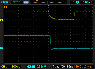
I am using EPWM (no HRPWM) with deadband, using ePWMxA as input to both RED and FED (twice as long as RED) and active high outputs.
When OutA falls, there is always a one clock low pulse (exactly 200nS) on OutB and then FED continues normally.
Please see picture. OutA is on top, OutB on bottom.
I tried to use separate A/B inputs, inverted inputs and outputs and anytime the output is active high, the pulse was there.
When OutB is set to active low, the pulse is not there probably because it is also low.
Any ideas what it is and how to get rid of it?
Martin
I do believe this is a configuration issue on the application code. Let me see if this has been answered before.
I have tried playing with registers but none could get rid of this pulse.
For now I programmed output B to be complementary and then added external inverter to invert it back to positive.
This works but makes design more complicated and is a workaround instead of a fix.
Still looking for a confirmation from TI to what it the cause.
Here is the PWM initialization function (under development), the rest of the program controls the duty of PWM and takes care of errors.
void PWM_WPS_Init(int16_t n) { // Configure PWM for 30.303Khz (33uS period), @200Mhz CPU Clock, @100MHz EPWMCLK EPWMCLKDIV (2), in master mode PWM_1ch_CNF(n, PWM_WPS_PRD, 1, 0); // Commented out code done by the macro above // (*ePWM[n]).TBCTL.bit.PRDLD = TB_IMMEDIATE; // set TB_IMMEDIATE load vs. TB_SHADOW // (*ePWM[n]).TBPRD = PWM_WPS_PRD-1; // EPWMCLKDIV (2), HSPCLKDIV (1), CLKDIV (1) set to 200MHz/2 = 100MHz frequency to get 30.303kHz PWM (TBPRD=3300) // (*ePWM[n]).TBPHS.bit.TBPHS = 0; // (*ePWM[n]).TBCTR = 0; // (*ePWM[n]).TBCTL.bit.CTRMODE = TB_COUNT_UP; // (*ePWM[n]).TBCTL.bit.HSPCLKDIV = HSPCLK_DIV1; // (*ePWM[n]).TBCTL.bit.CLKDIV = CLK_DIV1; // (*ePWM[n]).TBCTL.bit.PHSEN = TB_DISABLE; // (*ePWM[n]).TBCTL.bit.SYNCOSEL = TB_CTR_ZERO; // sync "down-stream" // Counter Compare Submodule Registers // (*ePWM[n]).CMPA.bit.CMPA = 0; // set duty 0% initially // (*ePWM[n]).CMPB.bit.CMPB = 0; // (*ePWM[n]).CMPCTL.bit.SHDWAMODE = CC_SHADOW; // (*ePWM[n]).CMPCTL.bit.LOADAMODE = CC_CTR_PRD; // Action Qualifier SubModule Registers // (*ePWM[n]).AQCTLA.bit.ZRO = AQ_SET; // (*ePWM[n]).AQCTLA.bit.CAU = AQ_CLEAR; (*ePWM[n]).AQTSRCSEL.bit.T1SEL = 0; // Use DCAEVT1 as the trigger for T1, for ramp signal comparator to control PWM output pulse width (*ePWM[n]).AQTSRCSEL.bit.T2SEL = 1; // Use DCAEVT2 as the trigger for T2, for ramp signal comparator to control PWM output pulse width (*ePWM[n]).AQCTLA2.bit.T1U = AQ_CLEAR; (*ePWM[n]).AQCTLA2.bit.T2U = AQ_CLEAR; // (*ePWM[n]).AQCTLB.bit.ZRO = AQ_NO_ACTION; // AQ_CLEAR for inverted output B (w/o dead-band) // (*ePWM[n]).AQCTLB.bit.CAU = AQ_NO_ACTION; // AQ_SET // (*ePWM[n]).AQCTLB.bit.PRD = AQ_NO_ACTION; // Setup dead-band registers (*ePWM[n]).DBCTL.bit.IN_MODE = DBA_ALL; // EPWMxA is the source for both delays (*ePWM[n]).DBCTL.bit.OUT_MODE = DB_FULL_ENABLE; // Enable Dead-band module (*ePWM[n]).DBCTL.bit.POLSEL = DB_ACTV_HIC; // Active High complementary (*ePWM[n]).DBCTL.bit.HALFCYCLE = 0; // Half Cycle Clocking Enable? (*ePWM[n]).DBCTL.bit.LOADREDMODE = 0b01; // Active DBRED Load Mode, 00: Load on Counter = 0 (CNT_eq), 01: Load on Counter = Period (PRD_eq) (*ePWM[n]).DBCTL.bit.LOADFEDMODE = 0b01; // Active DBFED Load Mode, 10: Load on either Counter = 0, or Counter = Period, 11: Freeze (no loads possible) (*ePWM[n]).DBCTL.bit.SHDWDBREDMODE = 1; // DBRED Block Operating Mode (*ePWM[n]).DBCTL.bit.SHDWDBFEDMODE = 1; // DBFED Block Operating Mode (*ePWM[n]).DBCTL.bit.OUTSWAP = 0b00; // Dead Band Output Swap Control (*ePWM[n]).DBCTL.bit.DEDB_MODE = 0; // Dead Band Dual-Edge B Mode Control (*ePWM[n]).DBRED.all = 20; // RED = 20 TBCLKs (~200 nS) (*ePWM[n]).DBFED.all = 40; // FED = 40 TBCLKs (~400 nS) // Enable CNT_zero interrupt using EPWMn Time-base (*ePWM[n]).CMPC = PWM_WPS_PRD-300; // This CMPC value allows enough time (3uS) to perform new loop calculation and update the control action before the end of the PWM cycle. (*ePWM[n]).ETSEL.bit.INTSEL = ET_CTRU_CMPA; // Use CTR = CMPC/CMPA (CMPC selected in the next line of code) (*ePWM[n]).ETSEL.bit.INTSELCMP = 1; // Enable event when CTR = CMPC (*ePWM[n]).ETPS.bit.INTPRD = ET_1ST; // Generate INT on every event (*ePWM[n]).ETCLR.bit.INT = 1; // Enable more interrupts (*ePWM[n]).ETSEL.bit.INTEN = 1; // Enable EPWM?INT generation // We also use comparators for OC protection. // Use ADC for current reading and also use PPB limits for additional OC protection (*ePWM[n]).CMPD = 200; // This CMPD value allows enough time (2uS) to stabilize after PWM pulse start. (*ePWM[n]).ETSEL.bit.SOCASEL = ET_CTRU_CMPB; // Use CTR = CMPD/CMPB (CMPD selected in the next line of code) (*ePWM[n]).ETSEL.bit.SOCASELCMP = 1; // Enable event when CTR = CMPD (*ePWM[n]).ETPS.bit.SOCAPRD = ET_1ST; // Generate SOC on every event (*ePWM[n]).ETCLR.bit.SOCA = 1; // Clear ETFLG[SOCA] (*ePWM[n]).ETSEL.bit.SOCAEN = 1; // Start of Conversion Enable // Setup comparators { // use COMPL for O.C. detection, COMPH for variable comparisons (i.e. current regulation, etc.) (*ePWM[n]).rsvd2[0] = 2; // EPWMSYNCOUTEN.bit.ZEROEN = 1; // Sync Cmpss with PWM Cmpss_Init(&Cmpss1Regs, 3275, 3275); // Enable CMPSS for driver over-current Cmpss_Init(&Cmpss4Regs, 2048, 2048); // Enable CMPSS for output control and over-current detection EALLOW; // Ramp for current loop setup Cmpss4Regs.CTRIPLFILCLKCTL.bit.CLKPRESCALE = 0; // set time between samples, max : 1023 at 200 MHz clock Cmpss4Regs.CTRIPLFILCTL.bit.SAMPWIN = 31; // # of samples in window, max : 31 Cmpss4Regs.CTRIPLFILCTL.bit.THRESH = 25; // recommended : thresh > sampwin/2 Cmpss4Regs.CTRIPLFILCTL.bit.FILINIT = 1; // Init samples to filter input value // Cmpss4Regs.COMPSTSCLR.bit.LSYNCCLREN = 1; // Enable PWMSYNC reset of comparator digital filter output latch // TODO: testing values Cmpss4Regs.RAMPMAXREFS = 0xFFFF; // 16-bit value for 2.5V input Cmpss4Regs.RAMPDECVALS = 0x0020; // 16-bit value at 200 MHz clock Cmpss4Regs.RAMPDLYS.bit.DELAY = 0x258; // 12-bit value at 200 MHz clock for 3uS delay Cmpss4Regs.COMPDACCTL.bit.RAMPSOURCE = n-1; Cmpss4Regs.COMPDACCTL.bit.RAMPLOADSEL = 0; // use latched RAMPMAXREFA value // Cmpss4Regs.COMPHYSCTL.bit.COMPHYS = 2; // COMP hysteresis set to 2x typical value (0-4 allowed for 0,12,24,36,48 CMPSS DAC LSB) // Cmpss4Regs.COMPDACCTL.bit.SWLOADSEL = 1; // DAC updated on PWMSYNC Cmpss4Regs.COMPDACCTL.bit.DACSOURCE = 1; // Ramp used Cmpss4Regs.CTRIPHFILCLKCTL.bit.CLKPRESCALE = 0; // set time between samples, max : 1023 at 200 MHz clock Cmpss4Regs.CTRIPHFILCTL.bit.SAMPWIN = 31; // # of samples in window, max : 31 Cmpss4Regs.CTRIPHFILCTL.bit.THRESH = 25; // recommended : thresh > sampwin/2 Cmpss4Regs.CTRIPHFILCTL.bit.FILINIT = 1; // Init samples to filter input value Cmpss4Regs.COMPSTSCLR.bit.HSYNCCLREN = 1; // Enable PWMSYNC reset of comparator digital filter output latch // OUTPUT1 sent to GPIO24 (pin 24) for testing OutputXbarRegs.OUTPUT1MUX0TO15CFG.all = 0x00000000; // select all cmpss tripL and tripH OutputXbarRegs.OUTPUT1MUX16TO31CFG.all = 0x00000000; OutputXbarRegs.OUTPUT1MUXENABLE.all = 0x00000080; // Enable Mux 7 to generate OUTPUT1 OutputXbarRegs.OUTPUTINV.bit.OUTPUT1 = 0; // XBAR output is NOT inverted OutputXbarRegs.OUTPUTLATCHENABLE.bit.OUTPUT1= 0; // XBAR output is NOT latched // Setup EPwmXbar to connect comparators to EPwm Digital Compare (DC) unit // Configure TRIP 4 to the O.C. trips from comparators 1,4, (7) EPwmXbarRegs.TRIP4MUX0TO15CFG.all = 0x00000000; // select all cmpss tripL and tripH EPwmXbarRegs.TRIP4MUX16TO31CFG.all = 0x00000000; EPwmXbarRegs.TRIP4MUXENABLE.all = 0x00000082; // Enable Mux 1,7,13 CMPSSx.CTRIPL to generate TRIP4 EPwmXbarRegs.TRIPOUTINV.bit.TRIP4 = 0; // XBAR output is NOT inverted // Setup EPwmXbar to connect comparators to EPwm Digital Compare (DC) unit // Configure TRIP 5 to the programable (ramp) trips from comparators (1,) 4, (7) EPwmXbarRegs.TRIP5MUX0TO15CFG.all = 0x00000000; // select all cmpss tripL and tripH EPwmXbarRegs.TRIP5MUX16TO31CFG.all = 0x00000000; EPwmXbarRegs.TRIP5MUXENABLE.all = 0x00000040; // Enable Mux 6 CMPSS4.CTRIPH to generate TRIP5 EPwmXbarRegs.TRIPOUTINV.bit.TRIP5 = 0; } EALLOW; // Setup Digital Comparator (DC) submodule to blank out switching noise periods (*ePWM[n]).DCFCTL.bit.SRCSEL = DC_SRC_DCAEVT1; (*ePWM[n]).DCFCTL.bit.BLANKE = DC_BLANK_ENABLE; (*ePWM[n]).DCFCTL.bit.BLANKINV = DC_BLANK_NOTINV; (*ePWM[n]).DCFCTL.bit.PULSESEL = DC_PULSESEL_ZERO_PRD; // (*ePWM[n]).DCFCTL.bit.EDGEFILTSEL = 0; // (*ePWM[n]).DCFCTL.bit.EDGEMODE = ; // (*ePWM[n]).DCFCTL.bit.EDGECOUNT = ; (*ePWM[n]).DCFOFFSET = 0; // at 100 MHz (TBCLK) (*ePWM[n]).DCFWINDOW = 300; // (3uS) in 10nS resolution to prevent over-current (DCAEVT1) tripping during switch pulse ringing // TODO: remove (*ePWM[n]).DCCAPCTL.bit.CAPE = 1; // Capture enable (for debugging) // Configure and enable all trip components (*ePWM[n]).DCTRIPSEL.bit.DCALCOMPSEL = DC_TRIPIN4; // Trip 4 is the input to the DCALCOMPSEL (*ePWM[n]).DCTRIPSEL.bit.DCAHCOMPSEL = DC_TRIPIN5; // Trip 5 is the input to the DCAHCOMPSEL // TODO: Filter? // (*ePWM[n]).DCACTL.bit.EVT1LATCLRSEL = 0; // (*ePWM[n]).DCACTL.bit.EVT1LATSEL = 0; (*ePWM[n]).DCACTL.bit.EVT1SRCSEL = DC_EVT_FLT; // or DC_EVT2; (*ePWM[n]).DCACTL.bit.EVT1FRCSYNCSEL = DC_EVT_ASYNC; (*ePWM[n]).TZDCSEL.bit.DCAEVT1 = TZ_DCAL_HI; // Digital Compare output event selection (*ePWM[n]).TZDCSEL.bit.DCAEVT2 = TZ_DCAH_HI; // (*ePWM[n]).TZSEL.bit.OSHT5 = TZ_ENABLE; // Enable TZ5 (clock fail) as One-shot trip source (*ePWM[n]).TZSEL.bit.OSHT6 = TZ_ENABLE; // Enable TZ6 (CPU EMUSTOP) as One-shot trip source // TODO: done in AQ module (*ePWM[n]).TZSEL.bit.DCAEVT1 = TZ_ENABLE; // Enable DCAEVT1 (over-currents) as One-shot trip source to clear PWM outputs // (*ePWM[n]).TZSEL.bit.DCAEVT2 = TZ_ENABLE; // Enable DCAEVT2 as CBC trip source // (*ePWM[n]).TZCTL.bit.DCAEVT1 = TZ_FORCE_LO; // EPWMx will go low on DCAEVT1 event // (*ePWM[n]).TZCTL.bit.DCAEVT2 = TZ_NO_CHANGE; // EPWMx will go low on DCAEVT2 event (*ePWM[n]).TZCTL.bit.TZA = TZ_FORCE_LO; // EPWMxA will go low on any trip event (*ePWM[n]).TZCTL.bit.TZB = TZ_FORCE_HI; // EPWMxB will go high on any trip event (*ePWM[n]).TZCLR.bit.OST = 1; // Clear any spurious OC trip (*ePWM[n]).TZCLR.bit.CBC = 1; (*ePWM[n]).TZCLR.bit.CBCPULSE = 0; // clear on CTR=ZERO(0), PRD(1), BOTH(2) (*ePWM[n]).TZCLR.bit.DCAEVT1 = 1; (*ePWM[n]).TZCLR.bit.DCAEVT2 = 1; (*ePWM[n]).TZCLR.bit.INT = 1; // Clear interrupt flag (*ePWM[n]).TZOSTCLR.bit.DCAEVT1 = 1; (*ePWM[n]).TZEINT.bit.OST = 1; // Trip zone interrupt select for OC detection EDIS; }
I'm not sure what is causing that drop to LOW from the time that the Falling edge occurs and the delay is applied. Subrahmanya do you know what can cause this?
Can you also disable the deadband, share a picture of the signals? They should be identical, correct?
I am out of the country and do not have access to the system for next two weeks but I know that without the deadband everything worked as expected.
I think it would be better for someone to duplicate the problem and verify it so that we know the problem is real and can be worked on in parallel.
Martin,
THis thread will be closing soon due to a lack of responses. If you are still working this feel free to respond here, and we will gladly help you out.
Regards,
Cody
The problem is still not resolved.
I do not have any ideas on what is wrong.
Unless some TI genius let's me know how to fix registers which I already provided, I consider it a MCU bug and expect TI to acknowledge it.
When I have some time I will try to use one of example codes to duplicate it.
Martin
Martin,
I understand your frustration, lets see what we can find out. This could be a bug, and if it is I will gladly acknowledge and document it. But at the same time I would like to say that the PWM module is very complex, and quite often an effect like this can be caused by another submodule. For this reason if you could duplicate it with an example that would be hugely helpful in determining the root cause. Similarly if you can determine that changing configuration X changes the behavior, that too can help me limit down what could be causing this.
A few questions that may help us get to the bottom of this:
One last thing, I want to reassure you that we are committed to getting to root cause on your issue, but it may take some back and forth.
Thanks,
Cody
In example code epwm_deadband_c28.c for F2837xS, 3 examples are included:
- ePWM1: Active low PWMs
- ePWM2: Active low complementary PWMs
- ePWM3: Active high complementary PWMs
There is no example for Active High PWMs. I wonder why?
Will modify it to verify.
As requested, here are the details:
1. I use Digital Compare Blanking window after transitions to prevent switching noise interference
2. When I disable RED/FED the glitch goes away. The glitch only happens in active high mode!
3. I only used up-count mode
4. CMPC/D values are fixed and not changing; used to trigger calculations and ADC conversions
period = 3300
CMPC = period-300; // allows enough time (3uS) to perform new loop calculation
CMPD = 200; // allows enough time (2uS) to stabilize after PWM pulse start
CMPA is changing between 300 and 1300 when CMPC triggers.
The glitch happens always exactly at start of FED for one clock pulse no matter what CMPA is.
Martin,
I implemented similar code and did not see the issue.
I then began updating my code to be as similar to yours as possible. In doing so I realized you are clocking the ePWM at 200MHz, can you confirm this is correct?
Please note that this device only has a 100MHz PWM module. When overclocking the PWM by 2 times the maximum frequency race conditions, similar to what you are seeing, are to be expected. Please update the EPWMCLKDIV bit of the PERCLKDIVSEL register to be equal to 1 and this problem should go away. This is the default upon reset, and we have added a few notes and cautions in the TRM to try and avoid this confusion. Finally the Datasheet will list the frequency maximum of the PWM at 100MHz.
If you absolutely need a 200MHz PWM TMS320F28388D is an option.
Regards,
Cody
Cody,
Thank you for the suggestion but I already checked that.
The CPU runs at 200 MHZ and I know that PWM needs and runs at 100 MHZ which is fine for my application.
I have following line in the initialization:
ClkCfgRegs.PERCLKDIVSEL.bit.EPWMCLKDIV = 1; // Reset defaults are /2 but make sure here again
Also when I set TBPRD to 3300 I get expected 30.303 kHz with enough resolution to control duty.
I think it must be something else.
Martin
I see where you are coming from.
It is true that the glitch is exactly 200 nS long and exactly at the beginning of FED delay and some clocking/race issue is suspected and I agree.
What is interesting that it only happens with active high pulses and is not noticeable with active low even though it could be present.
Martin,
OK, understood. I will try one more time to replicate this on my side. If I cannot replicate: It will be helpful if you could build a simple test case which shows the issue.
Regards,
Cody
I thought of something.
My PWM duty is controlled by the event generated by comparator+ramp+blanking.
This is attached to PWM with (from code above):
(*ePWM[n]).AQTSRCSEL.bit.T1SEL = 0; // Use DCAEVT1 as the trigger for T1, for ramp signal comparator to control PWM output pulse width
(*ePWM[n]).AQTSRCSEL.bit.T2SEL = 1; // Use DCAEVT2 as the trigger for T2, for ramp signal comparator to control PWM output pulse width
(*ePWM[n]).AQCTLA2.bit.T1U = AQ_CLEAR;
(*ePWM[n]).AQCTLA2.bit.T2U = AQ_CLEAR;
I am wandering if the comparator triggers the A & B outputs before the FED takes over couple of clocks later causing the glitch?
Martin
Martin,
the FED won't be able to force the PWM's output high again, it will only increase the amount time before the output is pulled low. However I think you might be on to something here. T1 and T2 are async, if a small pulse was missed by the blanking window it could cause a glitch on the PWM's output.
It doesn't look like I will have time to try and replicate your issue today, I should hopefully have time tomorrow.
Regards,
Cody
I could try this in couple of days.
Will also try changing this line to DC_EVT_SYNC:
(*ePWM[n]).DCACTL.bit.EVT1FRCSYNCSEL = DC_EVT_ASYNC;
The blanking is enabled at the beginning of the period for 3 uS to suppress FET switching on noise from reaching triggers (the PWM duty+DB is always > 3 uS)
// Setup Digital Comparator (DC) submodule to blank out switching noise periods
(*ePWM[n]).DCFCTL.bit.SRCSEL = DC_SRC_DCAEVT1;
(*ePWM[n]).DCFCTL.bit.BLANKE = DC_BLANK_ENABLE;
(*ePWM[n]).DCFCTL.bit.BLANKINV = DC_BLANK_NOTINV;
(*ePWM[n]).DCFCTL.bit.PULSESEL = DC_PULSESEL_ZERO_PRD;
(*ePWM[n]).DCFOFFSET = 0; // at 100 MHz (TBCLK)
(*ePWM[n]).DCFWINDOW = 300; // (3uS) in 10nS resolution to prevent over-current (DCAEVT1) tripping during switch pulse ringing
I do not understand what happened to my first reply to your question but I will continue (it probably got saved under different subject).
Today I tried changing:
(*ePWM[n]).DCACTL.bit.EVT1FRCSYNCSEL = DC_EVT_ASYNC;
to DC_EVT_SYNC
and
(*ePWM[n]).DBCTL.bit.HALFCYCLE = 0;
to 1 and back to 0
and none of them made any difference. However I zoomed in on the glitch and found the following:
- the glitch always starts 10 nS before FED delay starts or other words before CHAN A falls
- the glitch is exactly 160 (most of the time) or 170 nS (sometimes)
I think this is important information that there is 10 nS difference between falling edges which is exactly the width of the EPWMCLK and that the glitch width is 16(+1) clocks.
Any ideas what could it be?
I will try to disable some of the functions to look for clues.
Martin
Another thing I noticed is that the glitch does not have a steep falling edge like the TTL driven signal should have.
It seems like it is not driven but floating down (weak pull down?).
See picture; top is the glitch (170 nS width captured), bottom is the falling edge of CHAN A pulse (reversed channels of the original picture).
I can't think of naything that you first post points towards.
Martin Kajdas said:It seems like it is not driven but floating down (weak pull down?).
That might be a interesting conclusion... I don't think I would have thought of it that way.
Check if any part of the the TZ has been configured to put the PWM in a "high-impedance" state. If you have not configured it, it still may be forcing to high-impedance mode as this is the default configuration. For this reason please check the following device registers at run time when you see the issue happening.
DCBEVT2, DCBEVT1, and TZB. While you're checking this I would also check the DCAEVTy registers.
Regards,
Cody
I have disabled Digital Compare Submodule by changing the DCTRIPSEL register to an unused input and the PWM output became longer as expected but no glitch!
I think I can conclude that it is something in DC or TZ modules.
This is weird.
I put the DC module back and got the glitch back as expected. Then I paused the debugger and continued and the glitch disappeared but the PWM waveform was still correctly controlled by DC.
Then I restarted the CPU in debugger and the glitch came back. Seems that pausing the debugger fixes the glitch. Ooooo?
Eureka!
I still do not understand why debugger fixed it but I found real solution.
From the "floating" conclusion I realized that the TZCTL register is reset to floating by default.
I only programmed TZA and TZB bits to the values I wanted as I was using them for CBC and OSHT and left others in default state (floating).
When I programmed DCAEVTx and DCBEVTx to the same values as TZA and TZB, the glitch became nicely squared.
This made me realize that I need to program DCAEVTx and DCBEVTx to TZ_NO_CHANGE and the glitch disappeared.
After thinking about it, it makes some sense if I only knew how TZCTL register actually worked.
I can conclude that the explanation of the TZCTL register logic and the delays involved is very weak in the technical reference manual.
Martin
Martin,
Great I'm glad we could get your issue resolved!
Unfortunately, that is exactly what I was referring to in my last post. Sorry, I should have caught this issue earlier, but I was distracted by the fact that your issue changed with the DB control mode.
This is a reasonably common issue as the default behavior is to put the PWM's output into high-impedance mode. I agree that the TZ section is confusing and jumps around a lot. I am actually in middle of rewriting that entire section.
If you have any specific feedback on the information in the section, or new information that you think would be helpful to have in the section, that would be helpful for me.
Regards,
Cody
Cody,
My confusion regarding the documentation was due to lack of details regarding the EPWM trip logic and TZCTL register; it is a priority driven selector switch and that the DCAEVTx.force inputs have higher priority than EPWMxA and TZA inputs (makes sense but I was using DCAEVTx for TZA only and did not think of priorities).
The second issue was with the 160-170 nS delay between DCAEVTx.force signal and when it released control of the trip logic. I still do not understand it.
DCAEVTx.force signal was not latched by CMPSS so its pulse length should be calculated but I do not remember if there is enough information to do that so I do not know how it ended up with 160 nS.
My biggest mistake was the assumption that since I have EPWM with Deadband, that deadband pulse will never be interrupted by other priority signal. This should be clear to me not to be the case from the submodule block diagram but since the priorities were not defined in trip zone, I missed it completely.
I hope this helps.