This thread has been locked.
If you have a related question, please click the "Ask a related question" button in the top right corner. The newly created question will be automatically linked to this question.
Tool/software: Code Composer Studio
Hello everyone!
I face pretty strange behavior of mcu.
1. I set CSM password different from all ones
2. Then program mcu.
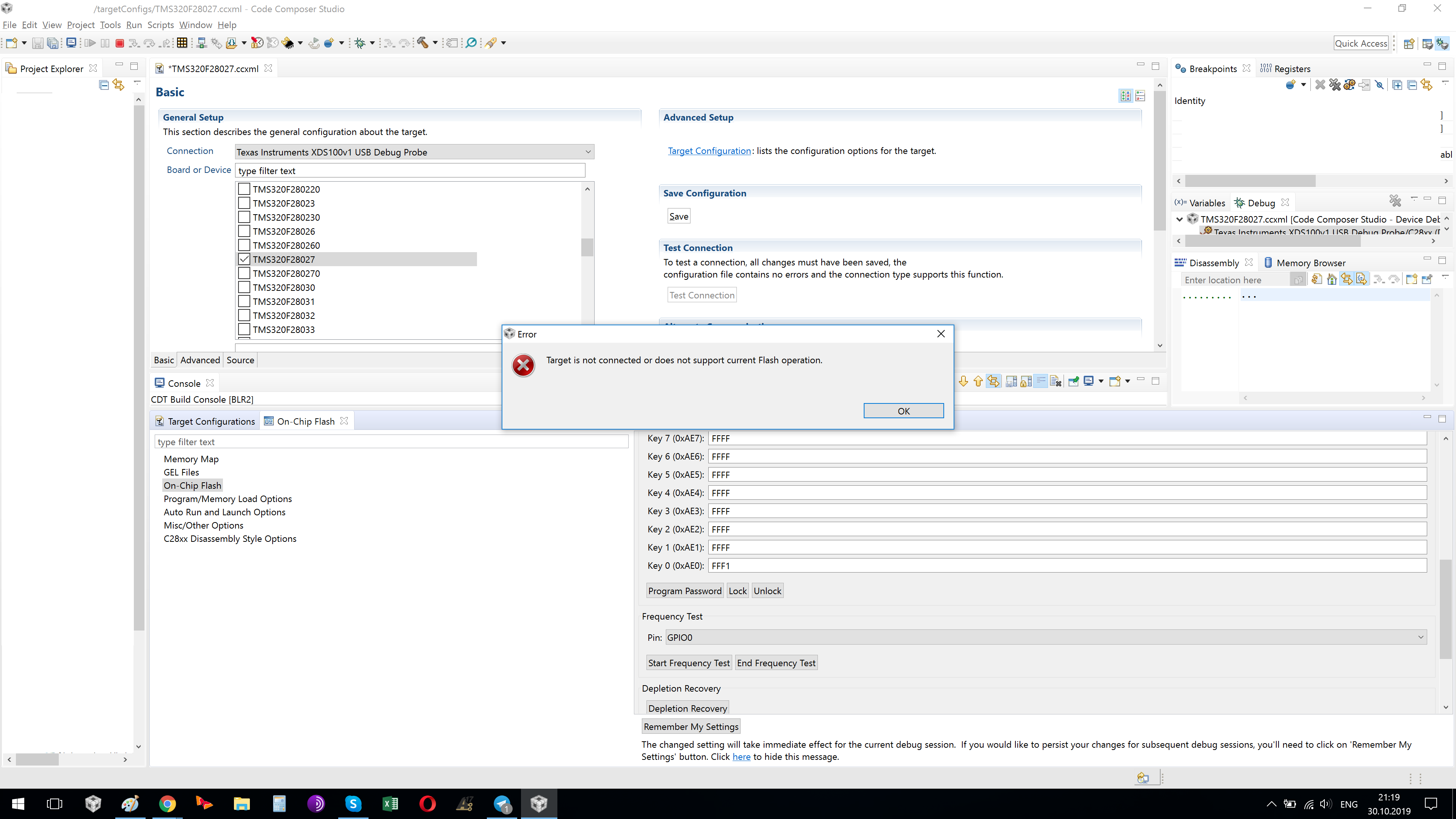
3. Then I tried to check if code protection works - I set wrong key in key register Properties->Debug->Flash settings, and in "Flash Program Setting" I set Verify Only
4. Then I start debug session and got in console window something like - ... GEL ..can't calibrate device... device is locked... e.t.c.
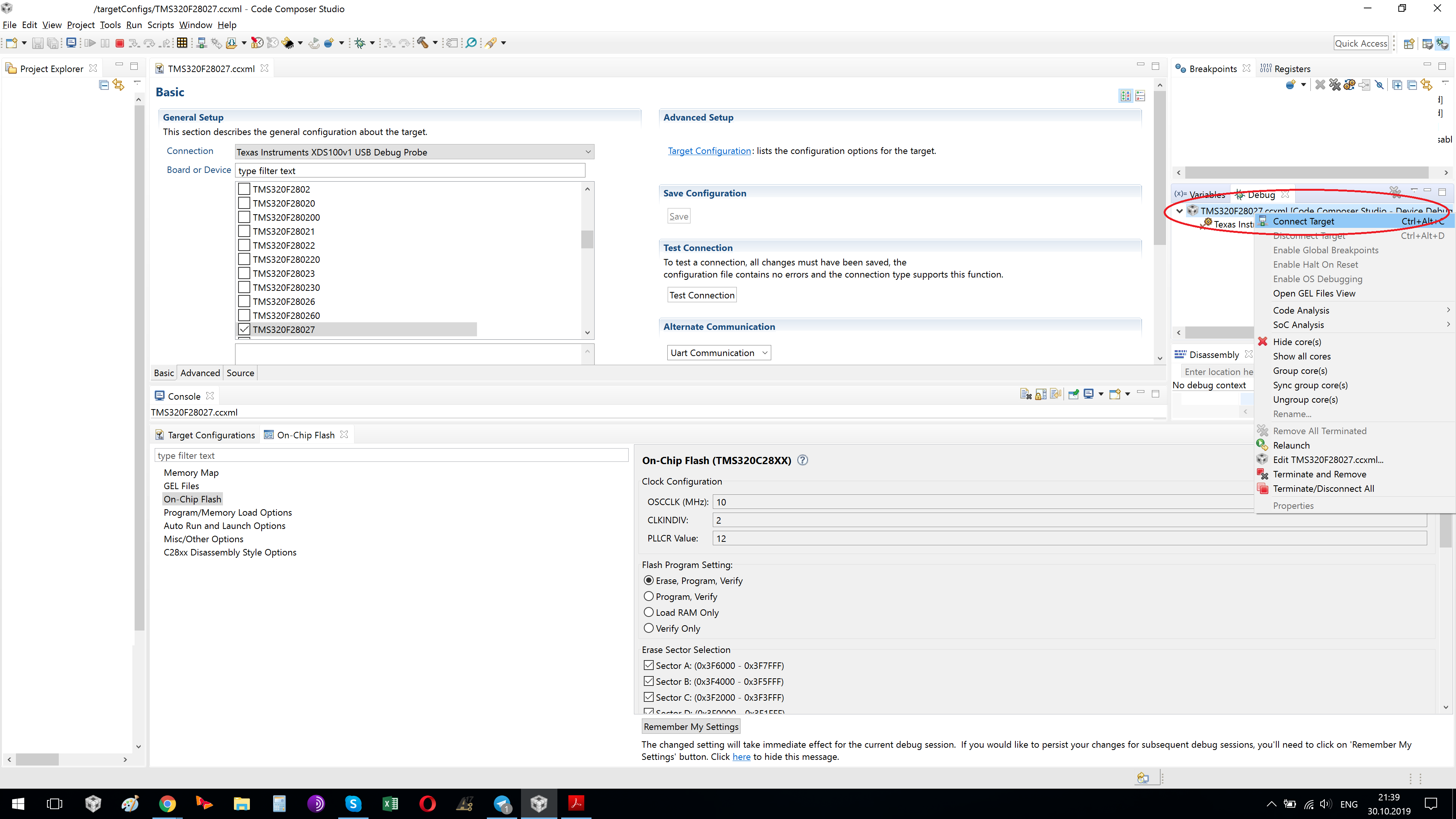
5. After that I can't connect to the mcu irrespectible of values in CSM keys.. And get "Error connecting to the target: (Error -1135 @ 0x0)" error...
This happens twice on two mcu's. Before setting CSM password everything was ok with connecting and debugging.
No reloading or resetting helps..
I'm using CCS Version: 8.3.0.00009, XDS100v1.
MCU works ok.
Hi,
I forwarded this thread to the C2000 device experts, but my tests done with another device and the same Debug Probe (XDS100v1) work well.
In this case, I suspect there may be intrinsic configurations relative to the device itself that I may be missing - thus I forwarded this thread.
Regards,
Rafael
Hi,
There is another strange issue I discovered before problems with CSM.
If mcu connected to the JTAG, it is not restart after reset. That is, - if i switch power off/on mcu does not restart.
It also does not restart in debug session when I press "reset mcu" button. In this case, disassembly shows that code enters infinite loop at
0x3FF6B4: AND AL, @0x1C, #0x8000 0x3FF6B6: LSR AL, 15 0x3FF6B7: CMPB AL, #0x1 0x3FF6B8: SBI -4, NEQ
AL = 0.
If I disconnect mcu from JTAG, it resets.
If it connected to the JTAG mcu runs only if I start debug session and reprogram code....
Please help!
Hi,
Is this a custom board or are you using a F2802x evaluation board made by TI?
What do you have the boot mode selection pins set to? Maybe try a different boot mode by configuring the GPIOs differently when running into the issue where you cannot connect:
I believe what you explained regarding the JTAG reset behavior before the CSM issue is expected and normal behavior.
Best,
Kevin
Hi, Kevin
I've tried next setups:
1. custom mcu board + custom JTAG programmer + Boot to flash mode / Parallel IO mode.
2. commercial mcu board + custom JTAG programmer + Boot to flash mode.
3. TMS320C2000 Experimerter Kit with 28027 controlCard.
In all 3 cases results are the same.
I've tried on another laptop, also I tried with another USB cable... The result is the same - after programming CSM i can't connect to the mcu..
Here is the message from console at very first try to enter debug after burning CSM password
-------------------------
C28xx: GEL Output: Device Calibration not complete, check if device is unlocked and recalibrate.C28xx: Flash Programmer: Warning: The configured device (TMS320F28027), does not match the detected device (). Flash Programming operations could be affected. Please consider modifying your target configuration file. C28xx: GEL Output: Device Calibration not complete, check if device is unlocked and recalibrate.C28xx: File Loader: Verification failed: Values at address 0x3F6CF3@Program do not match Please verify target memory and memory map. C28xx: GEL: File: C:\Users.........\xxx.out: a data verification error occurred, file load failed. C28xx: Verification-Only step completed.
--------------------------
Also here is CSM file
; code security module. .sect "csmpasswds" .int 0xFFF1 ;PWL0 (LSW of 128-bit password) .int 0xFFFF ;PWL1 .int 0xFFFF ;PWL2 .int 0xFFFF ;PWL3 .int 0xFFFF ;PWL4 .int 0xFFFF ;PWL5 .int 0xFFFF ;PWL6 .int 0xFFFF ;PWL7 (MSW of 128-bit password) ;---------------------------------------------------------------------- ; For code security operation, all addresses between 0x3F7F80 and ; 0X3f7ff5 cannot be used as program code or data. These locations ; must be programmed to 0x0000 when the code security password locations ; (PWL) are programmed. If security is not a concern, then these addresses ; can be used for code or data. ; The section "csm_rsvd" can be used to program these locations to 0x0000. .sect "csm_rsvd" .loop (3F7FF5h - 3F7F80h + 1) .int 0x0000 .endloop ;//=========================================================================== ;// End of file. ;//===========================================================================
and there is my cmd file
MEMORY { PAGE 0: /* Program Memory */ /* Memory (RAM/FLASH/OTP) blocks can be moved to PAGE1 for data allocation */ //PRAML0 : origin = 0x008000, length = 0x000800 /* on-chip RAM block L0 */ //L0PROGRAM : origin = 0x008000, length = 0x000100 // bilo 200hex 512 dlya super fast koda i dlya raboti s FLASH L0PROGRAM : origin = 0x008000, length = 0x000600 // tak, potomu chto ne vlazit teper flash api. ili ispolzovat iz ROM, no // no nuzhno //INIT_PIPELINE_RAM : origin = 0x008000, length = 0x00000A // run from RAM dlya vkl pipeline. Glavnoe chtob c_int00 tuda nichego ne napisal // potom na mesto INIT_PIPELINE zapishetsya chto-to. no nam ne vazhno, t.k. ona vizivaetsya tolko raz i potom ne nuzhna OTP : origin = 0x3D7800, length = 0x000400 /* on-chip OTP */ FLASHA : origin = 0x3F2000, length = 2*0x002000+0x001000 //0x001F80+0x002000*2 /* on-chip FLASH */ //INIT_PIPELINE_ROM : origin = 0x3F2000, length = 0x00000A//;0x000020 // load to ROM & run from RAM dlya vkl pipeline //FLASHC : origin = 0x3F2000, length = 0x002000 /* on-chip FLASH */ //FLASHB : origin = 0x3F4000, length = 0x002000 /* on-chip FLASH */ //FLASHA : origin = 0x3F6000, length = 0x001F80 /* on-chip FLASH */ CSM_RSVD : origin = 0x3F7F80, length = 0x000076 /* Part of FLASHA. Program with all 0x0000 when CSM is in use. */ BEGIN : origin = 0x3F7FF6, length = 0x000002 /* Part of FLASHA. Used for "boot to Flash" bootloader mode. */ CSM_PWL_P0 : origin = 0x3F7FF8, length = 0x000008 /* Part of FLASHA. CSM password locations in FLASHA */ IQTABLES : origin = 0x3FE000, length = 0x000B50 /* IQ Math Tables in Boot ROM */ IQTABLES2 : origin = 0x3FEB50, length = 0x00008C /* IQ Math Tables in Boot ROM */ IQTABLES3 : origin = 0x3FEBDC, length = 0x0000AA /* IQ Math Tables in Boot ROM */ ROM : origin = 0x3FF27C, length = 0x000D44 /* Boot ROM */ RESET : origin = 0x3FFFC0, length = 0x000002 /* part of boot ROM */ VECTORS : origin = 0x3FFFC2, length = 0x00003E /* part of boot ROM */ PAGE 1 : /* Data Memory */ /* Memory (RAM/FLASH/OTP) blocks can be moved to PAGE0 for program allocation */ /* Registers remain on PAGE1 */ BOOT_RSVD : origin = 0x000000, length = 0x000050 /* Part of M0, BOOT rom will use this for stack */ RAMM0 : origin = 0x000050, length = 0x0003B0 /* on-chip RAM block M0 */ RAMM1 : origin = 0x000400, length = 0x000400 /* on-chip RAM block M1 */ //----- from DSP2802x_Headers_nonBIOS.cmd - nuzho dlya Si koda DEV_EMU : origin = 0x000880, length = 0x000105 /* device emulation registers */ SYS_PWR_CTL : origin = 0x000985, length = 0x000003 /* System power control registers */ FLASH_REGS : origin = 0x000A80, length = 0x000060 /* FLASH registers */ CSM : origin = 0x000AE0, length = 0x000010 /* code security module registers */ ADC_RESULT : origin = 0x000B00, length = 0x000020 /* ADC Results register */ CPU_TIMER0 : origin = 0x000C00, length = 0x000008 /* CPU Timer0 registers */ CPU_TIMER1 : origin = 0x000C08, length = 0x000008 /* CPU Timer0 registers (CPU Timer1 & Timer2 reserved TI use)*/ CPU_TIMER2 : origin = 0x000C10, length = 0x000008 /* CPU Timer0 registers (CPU Timer1 & Timer2 reserved TI use)*/ PIE_CTRL : origin = 0x000CE0, length = 0x000020 /* PIE control registers */ PIE_VECT : origin = 0x000D00, length = 0x000100 /* PIE Vector Table */ COMP1 : origin = 0x006400, length = 0x000020 /* Comparator 1 registers */ COMP2 : origin = 0x006420, length = 0x000020 /* Comparator 2 registers */ EPWM1 : origin = 0x006800, length = 0x000040 /* Enhanced PWM 1 registers */ EPWM2 : origin = 0x006840, length = 0x000040 /* Enhanced PWM 2 registers */ EPWM3 : origin = 0x006880, length = 0x000040 /* Enhanced PWM 3 registers */ EPWM4 : origin = 0x0068C0, length = 0x000040 /* Enhanced PWM 4 registers */ ECAP1 : origin = 0x006A00, length = 0x000020 /* Enhanced Capture 1 registers */ GPIOCTRL : origin = 0x006F80, length = 0x000040 /* GPIO control registers */ GPIODAT : origin = 0x006FC0, length = 0x000020 /* GPIO data registers */ GPIOINT : origin = 0x006FE0, length = 0x000020 /* GPIO interrupt/LPM registers */ SYSTEM : origin = 0x007010, length = 0x000020 /* System control registers */ SPIA : origin = 0x007040, length = 0x000010 /* SPI-A registers */ SCIA : origin = 0x007050, length = 0x000010 /* SCI-A registers */ NMIINTRUPT : origin = 0x007060, length = 0x000010 /* NMI Watchdog Interrupt Registers */ XINTRUPT : origin = 0x007070, length = 0x000010 /* external interrupt registers */ ADC : origin = 0x007100, length = 0x000080 /* ADC registers */ I2CA : origin = 0x007900, length = 0x000040 /* I2C-A registers */ CSM_PWL : origin = 0x3F7FF8, length = 0x000008 /* Part of FLASHA. CSM password locations. */ PARTID : origin = 0x3D7FFF, length = 0x000001 /* Part ID register location */ //----- end from DSP2802x_Headers_nonBIOS.cmd //L0SARAM : origin = 0x008100, length = 0x000C00 // (do 13.08.18 bilo 8200 i length b00) 2816 dlya dannih L0SARAM : origin = 0x008600, length = 0x000900 // 1792 dlya dannih L0STACK : origin = 0x008F00, length = 0x000100 // 768 dlya steka. == tomu chto v setupe compilera. Teper 256 dlya steka. //DRAML0 : origin = 0x008800, length = 0x000800 /* on-chip RAM block L0 */ BL_EEPROM :origin = 0x3F0000, length = 0x002000 /* on-chip FLASH. SECTOR D (sm. tms320f28027.pdf, p20) Ispolzuem dlya hraneniya nastraivaemih znacheniy */ //FLASHD : origin = 0x3F0000, length = 0x002000 /* on-chip FLASH */ FLASHD : origin = 0x3F7000, length = 0x000F80 /* on-chip FLASH */ //FLASHB : origin = 0x3F4000, length = 0x002000 /* on-chip FLASH */ } /* Allocate sections to memory blocks. Note: codestart user defined section in DSP28_CodeStartBranch.asm used to redirect code execution when booting to flash ramfuncs user defined section to store functions that will be copied from Flash into RAM */ SECTIONS { //----- from DSP2802x_Headers_nonBIOS.cmd - nuzho dlya Si koda /*** PIE Vect Table and Boot ROM Variables Structures ***/ // - s etim razobratsya /* UNION : > PIE_VECT, PAGE = 1 { BootVarsFile PieVectTableFile //eto moya takaya strochka.. x.z. budet li tam raspolagatsya Bl_cpu_scale_factor_sect : RUN = 0x000D04 //0x4 }*/ //vot eto v fayle nashel vmesto togo chto vishe... /*** PIE Vect Table and Boot ROM Variables Structures ***/ UNION run = PIE_VECT, PAGE = 1 { PieVectTableFile GROUP { EmuKeyVar EmuBModeVar FlashCallbackVar //dolzhno bit po adresu 0x000D02 - kak eto poluchaetsya?? FlashScalingVar //dolzhno bit po adresu 0x000D04 } } /*** Peripheral Frame 0 Register Structures ***/ DevEmuRegsFile : > DEV_EMU, PAGE = 1 SysPwrCtrlRegsFile : > SYS_PWR_CTL, PAGE = 1 //novoe dobavilos FlashRegsFile : > FLASH_REGS, PAGE = 1 CsmRegsFile : > CSM, PAGE = 1 AdcResultFile : > ADC_RESULT, PAGE = 1 CpuTimer0RegsFile : > CPU_TIMER0, PAGE = 1 CpuTimer1RegsFile : > CPU_TIMER1, PAGE = 1 CpuTimer2RegsFile : > CPU_TIMER2, PAGE = 1 PieCtrlRegsFile : > PIE_CTRL, PAGE = 1 /*** Peripheral Frame 1 Register Structures ***/ ECap1RegsFile : > ECAP1 PAGE = 1 GpioCtrlRegsFile : > GPIOCTRL PAGE = 1 GpioDataRegsFile : > GPIODAT PAGE = 1 GpioIntRegsFile : > GPIOINT PAGE = 1 /*** Peripheral Frame 2 Register Structures ***/ SysCtrlRegsFile : > SYSTEM, PAGE = 1 SpiaRegsFile : > SPIA, PAGE = 1 SciaRegsFile : > SCIA, PAGE = 1 NmiIntruptRegsFile: > NMIINTRUPT, PAGE = 1 XIntruptRegsFile : > XINTRUPT, PAGE = 1 AdcRegsFile : > ADC, PAGE = 1 I2caRegsFile : > I2CA, PAGE = 1 /*** Peripheral Frame 3 Register Structures ***/ Comp1RegsFile : > COMP1, PAGE = 1 Comp2RegsFile : > COMP2, PAGE = 1 EPwm1RegsFile : > EPWM1 PAGE = 1 EPwm2RegsFile : > EPWM2 PAGE = 1 EPwm3RegsFile : > EPWM3 PAGE = 1 EPwm4RegsFile : > EPWM4 PAGE = 1 /*** Code Security Module Register Structures ***/ CsmPwlFile : > CSM_PWL, PAGE = 1 /*** Device Part ID Register Structures ***/ PartIdRegsFile : > PARTID, PAGE = 1 //----- end from DSP2802x_Headers_nonBIOS.cmd /* Allocate program areas: */ .cinit : > FLASHA PAGE = 0 .pinit : > FLASHA, PAGE = 0 .text : > FLASHA PAGE = 0 .BL_START : load = (BEGIN, PAGE 0) //codestart : > BEGIN PAGE = 0 //.BL_INIT_PIPELINE : load = (FLASHA, PAGE 0) run = (INIT_PIPELINE_RAM, PAGE 0) //.BL_INIT_PIPELINE : load = (INIT_PIPELINE_ROM, PAGE 0) run = (INIT_PIPELINE_RAM, PAGE 0) BL_EEPROM_SECT : LOAD = BL_EEPROM, PAGE = 1 ramfuncs : LOAD = FLASHA, RUN = L0PROGRAM, //RUN = PRAML0, LOAD_START(_RamfuncsLoadStart), //LOAD_START(_Flash28_API_LoadStart), LOAD_END(_RamfuncsLoadEnd), //LOAD_END(_Flash28_API_LoadEnd), RUN_START(_RamfuncsRunStart), //RUN_START(_Flash28_API_RunStart), PAGE = 0 /* FlashFuncs : LOAD = FLASHA, RUN = L0PROGRAM, //RUN = PRAML0, //LOAD_START(_RamfuncsLoadStart), LOAD_START(_Flash28_API_LoadStart), //LOAD_END(_RamfuncsLoadEnd), LOAD_END(_Flash28_API_LoadEnd), //RUN_START(_RamfuncsRunStart), RUN_START(_Flash28_API_RunStart), PAGE = 0 */ /* Allocate program areas: */ /* The Flash API functions can be grouped together as shown below. The defined symbols _Flash28_API_LoadStart, _Flash28_API_LoadEnd and _Flash28_API_RunStart are used to copy the API functions out of flash memory and into SARAM */ /******************************************************************/ /* For Piccolo B we dont need to copy the API from Flash as it is */ /* present in BOOT ROM */ /******************************************************************/ Flash28_API: { -lFlash2802x_API_V201.lib(.text) -lFlash2802x_API_V201.lib(.econst) } LOAD = FLASHA, //LOAD = FLASHD, RUN = L0PROGRAM, //RUN = PRAML0, LOAD_START(_Flash28_API_LoadStart), LOAD_END(_Flash28_API_LoadEnd), RUN_START(_Flash28_API_RunStart), PAGE = 0 //csmpasswds : > CSM_PWL PAGE = 1 csmpasswds : > CSM_PWL_P0 PAGE = 0 csm_rsvd : > CSM_RSVD PAGE = 0 /* Allocate uninitalized data sections: */ .stack : > L0STACK PAGE = 1 //.stack : > RAMM0 PAGE = 1 //.ebss : > DRAML0 PAGE = 1 //.esysmem : > DRAML0 PAGE = 1 .ebss : > L0SARAM PAGE = 1 .esysmem : > L0SARAM PAGE = 1 /* Initalized sections go in Flash */ /* For SDFlash to program these, they must be allocated to page 0 */ //.econst : > FLASHA PAGE = 0 //.switch : > FLASHA PAGE = 0 .econst : > FLASHD PAGE = 1 .switch : > FLASHD PAGE = 1 /* Allocate IQ math areas: */ IQmath : > FLASHA PAGE = 0 /* Math Code */ IQmathTables : > IQTABLES, PAGE = 0, TYPE = NOLOAD /* Uncomment the section below if calling the IQNexp() or IQexp() functions from the IQMath.lib library in order to utilize the relevant IQ Math table in Boot ROM (This saves space and Boot ROM is 1 wait-state). If this section is not uncommented, IQmathTables2 will be loaded into other memory (SARAM, Flash, etc.) and will take up space, but 0 wait-state is possible. */ /* IQmathTables2 : > IQTABLES2, PAGE = 0, TYPE = NOLOAD { IQmath.lib<IQNexpTable.obj> (IQmathTablesRam) } */ /* Uncomment the section below if calling the IQNasin() or IQasin() functions from the IQMath.lib library in order to utilize the relevant IQ Math table in Boot ROM (This saves space and Boot ROM is 1 wait-state). If this section is not uncommented, IQmathTables2 will be loaded into other memory (SARAM, Flash, etc.) and will take up space, but 0 wait-state is possible. */ /* IQmathTables3 : > IQTABLES3, PAGE = 0, TYPE = NOLOAD { IQmath.lib<IQNasinTable.obj> (IQmathTablesRam) } */ /* .reset is a standard section used by the compiler. It contains the */ /* the address of the start of _c_int00 for C Code. /* /* When using the boot ROM this section and the CPU vector */ /* table is not needed. Thus the default type is set here to */ /* DSECT */ .reset : > RESET, PAGE = 0, TYPE = DSECT vectors : > VECTORS PAGE = 0, TYPE = DSECT }
Hi Konstantin,
Have you already tried unlocking the device with the passwords you set using the On-chip Flash tool within CCS?
Launch your target config file --> go to 'Tools' at the top of the debug mode --> select 'On Chip Flash' --> in the on-chip flash window scroll down to the "Code Security Password" section --> Enter in your passwords and click unlock
Let me know how that works.
Best,
Kevin
Hi Kevin,
Before unlocking device I have to establish a connection to it. (on chip flash window can be populated only after debug session has been started)
But I can't start a debug session due to error connection to the target...
As I understand correctly - if I flash mcu it should be no matter if it is locked or not. The Flash programmer just erases previous password and uses new one, right?
Konstantin,
You can connect to the target device and use the On-chip flash tool without starting an active debug session and loading code. Please follow the steps I mentioned above after launching the proper target config file and connecting to the device, i.e. right click C28x core and click connect to target.
Konstantin Shirokov said:As I understand correctly - if I flash mcu it should be no matter if it is locked or not. The Flash programmer just erases previous password and uses new one, right?
You cannot erase the flash if the device is locked. You must unlock it first with the programmed passwords.
Best,
Kevin
Konstantin,
OK, I see. You're 2nd post is what I was meaning when trying to connect to the device.
Can you try testing the connection of your target config and see if that works? Are you sure your debugger is a XDS100 v1 and not v2? Most of our evaluation boards use a v2 (though I know you said this is a custom board).
Best,
Kevin
Kevin,
Looks like i managed to connect to the mcu.
The issue was with boot option. If either or both switches of SW1 on ControlCARD turn off(any exept BootMode=GetMode) it connects to mcu and unlocks.
It looks strange, coz on my custom board i've tried all combinations with boot mode.
Also it's strange that there is not possible to connect to the locked target when using GetMode.
Below is what i get in console window. Is it ok that configured device does not match detected device? Also there is no difference wether i set up XDS100V1 or V2 in config.
C28xx: GEL Output:
Device Calibration not complete, check if device is unlocked and recalibrate.C28xx: Flash Programmer: Warning: The configured device (TMS320F28027), does not match the detected device (). Flash Programming operations could be affected. Please consider modifying your target configuration file.
C28xx: GEL Output:
Device Calibration not complete, check if device is unlocked and recalibrate.C28xx: GEL Output:
Device Calibration not complete, check if device is unlocked and recalibrate.
Hi Konstantin,
GetMode is configured to Boot from Flash by default, so that is likely why you cannot connect.
Konstantin Shirokov said:Below is what i get in console window. Is it ok that configured device does not match detected device?
The warning about the configured device appears when using the TMDSCNCD28027 and a target configuration that matches the F28027 device? This along with not being in getMode? I can't think of why that would happen if so, TMS320F28027 set in the target config matches the device correctly.
Best,
Kevin