This thread has been locked.

If you have a related question, please click the "Ask a related question" button in the top right corner. The newly created question will be automatically linked to this question.

TMS320F28069: Incomplete McBSP DMA transfers

Part Number: TMS320F28069

Hello,

I refer to the last question of the linked topic regarding McBSP DMA.

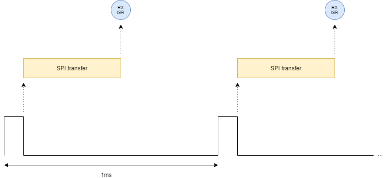
In our system, a SPI slave is connected to the C2000 McBSP module who acts as a SPI master (through McBSP). In a periodic manner (each 1ms), the slave requests the SPI master to start a SPI transfer using a GPIO (external interrupt). The number of bytes transferred is 12 bytes. The SPI transfer is handled by DMA and started in the EXTI interrupt (coming from the slave). Since the C2000 is also controlling a motor, the time spent in the EXTI ISR must be as short as possible (= McBSP + DMA transfer initialization and start must be optimal).

The problem is: if I initialize the DMA channel only once at startup, the first transfer is correct (12 bytes sent) but the next transfers are incomplete: the first 4 bytes are missing (only 8 bytes sent).

Do you have any idea if there is something more than re-enabling the DMA channels (RUN = 1) in order to re-start the complete transfer?

Here is the DMA configuration:

dma->DMACTRL |= (1 << 0);
asm(" nop");

// Channel 1: McBSPA transmit
// ----------------------------------------------------------

dma->CH1.BURST_SIZE = 1U;       // 2 16-bit word per burst
dma->CH1.SRC_BURST_STEP = 1;   // increment 1 16-bit addr. between words
dma->CH1.DST_BURST_STEP = 1;   // increment 1 16-bit addr. between words
dma->CH1.TRANSFER_SIZE = 2U;    // Interrupt every (2 + 1) bursts (= 12 bytes).

dma->CH1.SRC_TRANSFER_STEP = 1; // Move to next word in buffer after each word in a burst.
dma->CH1.DST_TRANSFER_STEP = 0xFFFF; // Decrement back to McBSP DXR2 register.

dma->CH1.SRC_ADDR_SHADOW = (uint32_t)&p_txBuf[0];
dma->CH1.SRC_BEG_ADDR_SHADOW = (uint32_t)&p_txBuf[0]; // TODO (S) : not needed - to be checked.
dma->CH1.DST_ADDR_SHADOW = (uint32_t)&obj->mcbspAHandle->DXR2;
dma->CH1.DST_BEG_ADDR_SHADOW = (uint32_t)&obj->mcbspAHandle->DXR2; // TODO (S) : not needed - to be checked.

// Clear sync error flag
dma->CH1.CONTROL |= (1U << 7);

// Set to maximum to avoid any source/destination wrap.
dma->CH1.SRC_WRAP_SIZE = 0xFFFFU;
dma->CH1.DST_WRAP_SIZE = 0xFFFFU;

//  dma->CH1.MODE |= (1U << 15); // Enable channel interrupt.
dma->CH1.MODE |= (1U << 9); // Generate interrupt at end of transfer.
dma->CH1.MODE |= (1U << 8); // Enable peripheral interrupt event.

dma->CH1.MODE |= (14U << 0); // DMA interrupt source: MXEVTA (McBSP transmission).

dma->CH1.CONTROL |= (1U << 4); // Clear any spurious interrupt flags.

// Channel 2: McBSPA receive
// ----------------------------------------------------------

dma->CH2.BURST_SIZE = 1U;       // 2 16-bit word per burst
dma->CH2.SRC_BURST_STEP = 1;   // increment 1 16-bit addr. between words
dma->CH2.DST_BURST_STEP = 1;   // increment 1 16-bit addr. between words
dma->CH2.TRANSFER_SIZE = 2U;    // Interrupt every (2 + 1) bursts (= 12 bytes).

dma->CH2.SRC_TRANSFER_STEP = 0xFFFF; // Decrement back to McBSP DRR2 register.
dma->CH2.DST_TRANSFER_STEP = 1; // Move to next word in buffer after each word in a burst.

dma->CH2.SRC_ADDR_SHADOW = (uint32_t)&obj->mcbspAHandle->DRR2;
dma->CH2.SRC_BEG_ADDR_SHADOW = (uint32_t)&obj->mcbspAHandle->DRR2; // TODO (S) : not needed - to be checked.
dma->CH2.DST_ADDR_SHADOW = (uint32_t)&p_rxBuf[0];
dma->CH2.DST_BEG_ADDR_SHADOW = (uint32_t)&p_rxBuf[0]; // TODO (S) : not needed - to be checked.

// Clear sync error flag
dma->CH2.CONTROL |= (1U << 7);

// Set to maximum to avoid any source/destination wrap.
dma->CH2.SRC_WRAP_SIZE = 0xFFFFU;
dma->CH2.DST_WRAP_SIZE = 0xFFFFU;

dma->CH2.MODE |= (1U << 15); // Enable channel interrupt.
dma->CH2.MODE |= (1U << 9); // Generate interrupt at end of transfer.
dma->CH2.MODE |= (1U << 8); // Enable peripheral interrupt event.

dma->CH2.MODE |= (15U << 0); // DMA interrupt source: MREVTA (McBSP reception).

dma->CH2.CONTROL |= (1U << 4); // Clear any spurious interrupt flags.

Here is the code used to re-start the transfer at each slave request:

ENABLE_PROTECTED_REGISTER_WRITE_MODE;
dma->CH1.CONTROL |= (1U << 0);
dma->CH2.CONTROL |= (1U << 0);
DISABLE_PROTECTED_REGISTER_WRITE_MODE;

Here is the first transfer (complete):

Here is the next transfer (missing bytes):

Regards

  • Johann,

    Can you send across your configuration for the McBSP registers.  I think the most important here is the XCR1/XCR2 and the SPCR2 registers.  I'm looking for how many bits you've specified in each transfer as when the McBSP is going to generate its interrupt.  I assume it is 16, but want to be sure.

    Also, have you set the continuous bit in the DMA Mode register(bit 11), or do you want to pause after a transfer completes and you service the X-mit ISR?

    Best,

    Matthew

  • Hello Matthew,

    MatthewPate said:

    I assume it is 16, but want to be sure.

    As you will see in the following configuration, we have set transfers to 32-bit for XWDLEN1 and RWDLEN1 in order to be as fast as possible. Even if it should maybe be 16-bit, I still do not get why it is working fine for the first transfer.

    Here is the McBSP registers configuration:

      HAL_Obj *obj = (HAL_Obj *)handle;
      McBSP_obj *mcbsp = (McBSP_obj *)obj->mcbspAHandle;
    
      // Step 1: place the transmitter and receiver in reset.
      // ----------------------------------------------------------
      mcbsp->SPCR2 &= ~MCBSP_SPCR2_XRST;
      mcbsp->SPCR1 &= ~MCBSP_SPCR1_RRST;
      // Step 2: place the sample rate generator in reset.
      // ----------------------------------------------------------
      mcbsp->SPCR2 &= ~MCBSP_SPCR2_GRST;
      // Step 3: program registers that affect SPI operation.
      // ----------------------------------------------------------
      mcbsp->SPCR1 |= (2 << MCBSP_SPCR1_CLKSTP_POS);  // Clock stop mode, without clock delay.
    
      // SPI mode 0 selection (low inactive state, McBSP transmit data on
      // the rising edge of SCLK and receives data on the falling edge.
      mcbsp->PCR &= ~MCBSP_PCR_CLKXP;
      mcbsp->PCR &= ~MCBSP_PCR_CLKRP;
    
      mcbsp->PCR |= (1U << MCBSP_PCR_CLKXM_POS);  // Clock is transmitted on the MCLKX pin.
    
      // Set the single-phase transmit/receive frame.
      mcbsp->XCR2 &= ~MCBSP_XCR2_XPHASE;
      mcbsp->RCR2 &= ~MCBSP_RCR2_RPHASE;
    
      // Set the transmit and receive frame length of 1 serial word.
      mcbsp->XCR1 &= ~MCBSP_XCR1_XFRLEN1;
      mcbsp->RCR1 &= ~MCBSP_RCR1_RFRLEN1;
    
      // Set the transmit and receive packet length to 32 bits.
      mcbsp->XCR1 |= (0x05 << MCBSP_XCR1_XWDLEN1_POS);
      mcbsp->RCR1 |= (0x05 << MCBSP_RCR1_RWDLEN1_POS);
    
      // Select LSPCLK as input clock for the sample rate generator.
      mcbsp->PCR &= ~MCBSP_PCR_SCLKME;
      mcbsp->SRGR2 |= MCBSP_SRGR2_CLKSM;
    
      // Divide-down the LSPCLK by 30 to get a CLKG frequency of 3 MHz.
      mcbsp->SRGR1 |= (MCBSP_CLKDV << MCBSP_SRGR1_CLKGDV_POS);
    
      // FSX pin is an output pin and used for chip select.
      mcbsp->PCR |= (1U << MCBSP_PCR_FSXM_POS);
    
      mcbsp->SRGR2 &= ~(1U << 12); // Frame sync. pulse on FSX pin.
    
      // FSX pin is active low.
      mcbsp->PCR |= MCBSP_PCR_FSXP;
    
      // SPI master operation requires fields XDATDLY and RDATDLY to be set to 1.
      mcbsp->XCR2 |= (1U << MCBSP_XCR2_XDATDLY_POS);
      mcbsp->RCR2 |= (1U << MCBSP_RCR2_RDATDLY_POS);

    Here is the code that disables the McBSP prior to configure and start the DMA again:

      mcbsp->SPCR2 &= ~(1U << 7);
      mcbsp->SPCR2 &= ~MCBSP_SPCR2_XRST;
      mcbsp->SPCR1 &= ~MCBSP_SPCR1_RRST;
      mcbsp->SPCR2 &= ~MCBSP_SPCR2_GRST;

    And here is the code that enables the McBSP after the DMA is configured and started:

      mcbsp->SPCR2 &= ~(1U << 7);
      mcbsp->SPCR2 &= ~MCBSP_SPCR2_XRST;
      mcbsp->SPCR1 &= ~MCBSP_SPCR1_RRST;
      mcbsp->SPCR2 &= ~MCBSP_SPCR2_GRST;

    Regarding the use case, we need to pause after the transfer completes and services the RX ISR as shown in the picture below:

    In the RX ISR, we read and process the data sent by the SPI slave.

    Regards,
    Johann

  • Johann,

    From the LA plot, we are missing 0xB0/A0/B1/A1, which I assume is the 1st 32-bit transfer that should happen.  Also we know we aren't off the SRC addresses, since we only get 2 transmissions vs a 3 with un-intended data(garbage from an un-initialized address nearby).

    I'd like to debug this by looking at the state of the DMA address registers (both the source and destination) for channel 1 when you have disabled the McBSP TX but both before and after you re-enable the DMA by setting the corresponding RUNSTS bit = 1.  

    I suspect that after the last transmission in 1st iteration the EVT signal from the McBSP to the DMA is still latched in the local DMA logic, so that as soon as you re-enable the DMA channel it attempts to write that initial word to the McBSP DXR2/1, but the McBSP has not yet been re-enabled so we miss it.  If you see the active src address = base +2 before you re-enable the McBSP then that would confirm this theory

    If we do see the above, perhaps we could change the trigger source of DMA channel 1 when the RUNSTS = 0 to something other than McBSP and then back again before setting RUNSTS = 1 to try and reset this local latch.

    Best,

    Matthew

  • Hello Matthew,

    MatthewPate said:
    From the LA plot, we are missing 0xB0/A0/B1/A1, which I assume is the 1st 32-bit transfer that should happen. 

    Yes, this should be the first 32-bit transfer. 

    Here are the DMA address registers of channel 1 before and after the DMA is enabled for the first time (correct transfer):

    • Before:
      • Source address: 0x00000000
      • Source address (shadow): 0x0000C01A
      • Destination address: 0x00000000
      • Destination address: 0x00005002
    • After:
      • Source address: 0x00000000
      • Source address (shadow): 0x0000C01A
      • Destination address: 0x00000000
      • Destination address: 0x00005002

    Here are the DMA address registers of channel 1 before and after the DMA is re-enabled (incomplete transfer):

    • Before:
      • Source address: 0x0000C020
      • Source address (shadow): 0x0000C01A
      • Destination address: 0x00005002
      • Destination address: 0x00005002
    • After:
      • Source address: 0x0000C01B
      • Source address (shadow): 0x0000C01A
      • Destination address: 0x00005002
      • Destination address: 0x00005002

    MatthewPate said:
    If we do see the above, perhaps we could change the trigger source of DMA channel 1 when the RUNSTS = 0 to something other than McBSP and then back again before setting RUNSTS = 1 to try and reset this local latch.

    I tried to set the trigger source of DMA channel 1 to "None":

    • In the DMA RX ISR  -> no effect
      ENABLE_PROTECTED_REGISTER_WRITE_MODE;
      m_halHandle->dmaHandle->CH1.MODE &= ~0x001FU;
      DISABLE_PROTECTED_REGISTER_WRITE_MODE;

    • Just before setting RUNSTS (none then McBSP source) -> no effect
    ENABLE_PROTECTED_REGISTER_WRITE_MODE;
    m_halHandle->dmaHandle->CH1.MODE &= ~0x001FU;
    m_halHandle->dmaHandle->CH1.MODE |= (14U << 0); // DMA interrupt source: MXEVTA (McBSP transmission).
    DISABLE_PROTECTED_REGISTER_WRITE_MODE;
    
    HAL_startMcBspADma(m_halHandle);

    Do you have any other idea?

    Regards

  • Johann,

    Thanks for running the experiment, I believe that the cause of this issue is what I had assumed in my last post.  We have to figure out how to clear the last interrupt event(McBSP ready X-mit).  From the above changing the source is not enough to clear the latch.

    I'm going to ask my colleagues in the design team to look into how the logic is constructed here, but I'd like to try some things in the meantime so we are not stuck.  If we find something that works, we can confirm with design this is the correct/repeatable behavior.

    There's two possibilities here, depending on if the signal from the McBSP is edge or level detect.  If its edge, then we should be able to clear the latch locally in the DMA.  If its level, then we need to understand how we can reset the signal local to the McBSP.

    1:DMA register modification) Instead of changing the PERINTSEL source, let's disable the peripheral interrupt by setting the PERINTE bit to 0, and then back to 1 before writing the RUNSTS bit.  This should definitely clear any local latch in the DMA.

    2:McBSP register modification) In between transfers lets put the transmitter into reset and out of reset by writing a "0" to the XRST bit in the SPCR2 register, then re-enabling by writing a "1".  Reading the TRM I don't believe this will reset your McBSP settings.

    Best,
    Matthew