This thread has been locked.

If you have a related question, please click the "Ask a related question" button in the top right corner. The newly created question will be automatically linked to this question.

Compatibility Launchpad F28379D / external Mode / Logg Data

Other Parts Discussed in Thread: INA250, TMDSCNCD28379D, TEST2, INA240, INA253, OPA320, INA293, ADS8860, THS4501
Hello,
I have a few questions around the Launchpad F28379D board:
1) Are the folowing TI product compatible with the Launchpad F28379D :
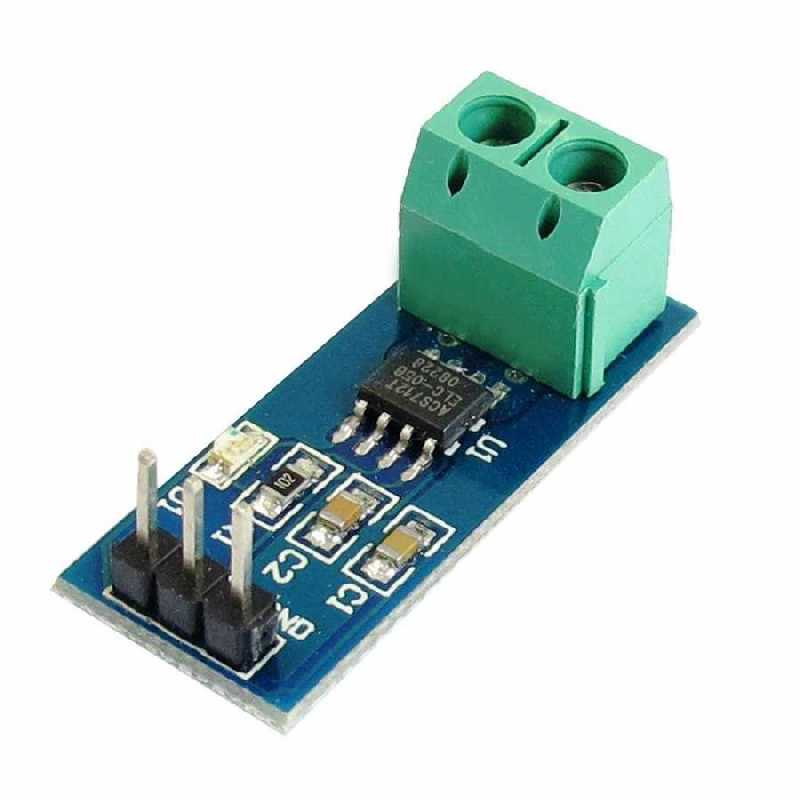
- current sensor : (INA250)   link : https://www.ti.com/tool/INA250EVM (49$)
- Mosfet driver  (UCC27423)   Link : https://www.ti.com/tool/UCC27423-4-5-Q1EVM (49$)
Is there any exemples or user documentation of the Launchpad F28379D and theses sensor/driver ??
2) I have a problem concerning the external operating mode of the Launchpad F28379D which does not start, I want to use it in simulink to run my program and at the same time send the data and save to a file (Host PC) ?
3)  I tried to read a 20kHz frequency signal from the analog input AIN_A0 of the Launchpad F28379D card and send it by the Simulink block (SCI_A), the signal is send but after a few seconds, the sending stops, an audible signal in the form of a beep is triggered to signal that the DSP card is disconnected and communication with the COM PORT with the HOST PC is stopped. How can I guarantee the continuity of communication through the serial COM port without any interruption ??
4) How can we use the USB-RS485 cable to communicate between the Launchpad F28379D card and the HOST PC (Simulink) ?
Thank you for help
  • Hassan,

    A1)There's no reason those devices can't be used with the C2000, but there is not any native PCB interconnects to mate with the Launch Pad pin headers, you would need to use wire wraps or feed into a universal bread board.  I would encourage you to look at the Industrial Application space to see if there is a ready made kit using a different platform(like the TMDSCNCD28379D) here https://www.ti.com/applications/industrial/overview.html 

    A2)I would first make sure that you can connect to Code Composer through the onboard XDS100v2 connection through the USB.  Make sure that JP1, JP2, JP3 are all populated as that brings the power from the USB connection to the F28379D MCU.  Once this is successful you should be able to connect to Simulink, but its easier to debug using CCS tools to find any issue

    A3)I'm not sure why the comms would stop, unless there was a high power noise interference, but that doesn't sound like the case.  I would ensure that the baud rate settings are consistent between the Simulink configurations and that of your host.

    A4)We have utilized a secondary channel on the FTDI chip on the LaunchPad to provide a UART connection between the F28379D and the USB connector.  If you open up a system device list on your PC host, you should see 2 ports enumerated when the launchpad is connected.  The primary is the debug probe, the other is this UART channel.  The only other configuration is that we need to make sure that the SCIA signals are coming out on GPIO42 and GPIO43.  Any example from TI, and likely MathWorks should have this configured already.

    Best,

    Matthew

  • Hello Matthew, 
    At the beginning I would like to thank you for your answer and for the diversity and richness of the information of your contribution.

    I would like to add some information to liven up our discussion:

    A1) for the first point which concerns compatibility, as you know it depends on the "principle of impedance adaptation" that we can make the connection
    between two circuits otherwise we can have a degradation or distortion of the signals because of the non compatibility between circuits,
    I only want to know and be sure if I order these two circuits they work well and are compatible with the F28379D card.

    A2) For the operating in external Mode, I have checked the JP1, JP2 and JP3 jumpers and are all installed in their places. How can i run extern mode from CCS?

    From simulink, I launched the external mode from menu:
    code ---> external mode control panel ---> connect, I received the following message:
    Could not execute target data map file 'test2_ert_rtw \ test2_targ_data_map' or it does not exist.
    Stop the target, delete the test2 executable, rebuild the code, and try again. Note that execution of external mode requires the build directory to be present  !!!

    For the extern mode test I put a PWM block and an ADC converter to record an analog signal (AIN_A5) in a "Scope", all settings are correct:
    TX ---> GPIO 42
    RX ---> GPIO 43
    Clocking = internal clock = 10MHz,
    External mode = COM4, ​​verbose checked.

    I received the following message:

    Error occurred while executing External Mode MEX-file 'ext_comm':
    Failed to connect to the target. A time-out occurred while waiting for the connection response from the target. Possible reasons for the time-out:
    a) The target is not switched on.
    b) The target is not connected to your host machine.
    c) The application for the model is not running on the target. You might have clicked the Stop button. If the Run button is not dimmed, click it. Otherwise, click the Build button, which downloads and runs your application on the target.

    When i removed the ADC block, and left only the PWM block and the constant source the external mode works !!!


    I changed in build option: CPU1 to CPU2, I got the following message:

    The model that you are trying to run in External mode does not match the application running on your target. Checksum test (TARGET_CONNECT) failed. The host model's structural checksum is [2414900011, 82752671, 4210689512, 1023461036] and the target application's structural checksum is [3174072407, 4041404685, 3703695784, 2097472781]. Rebuild the model, run it on your target, and start External mode simulation again. !!!!

    when I put both PWM and ADC blocks, the extern mode does not work !! here is the message I received:

    Error occurred while executing External Mode MEX-file 'ext_comm':
    Failed to connect to the target. A time-out occurred while waiting for the connection response from the target. Possible reasons for the time-out:
    a) The target is not switched on.
    b) The target is not connected to your host machine.
    c) The application for the model is not running on the target. You might have clicked the Stop button. If the Run button is not dimmed, click it. Otherwise, click the Build button, which downloads and runs your application on the target.

    A3 ) for point 3, the transfer via the COM3 port stops when I connect the PWM pin to the DC / DC converter gate. maybe you are right, how i can avoid the 
    noise interference produced by switching the power switch !!

    A4) for point 4 concerning the use of RS485 for data transfer from F28379D and the PC Host, I have not received a clear answer on this subject, 
    I see that the dsp card is equipped with serial output SCI_A, SCI_B , SCI_C I asked this question to know if possible while the the RS485 is characterized
    by the speed of data transfer?

    Thank you Matthew
  • Hassan,

    Q1)I believe that both the INA and UCC devices are fine to use with the C2000.

    For the UCC27243 there is a TI design that integrates both this and a C2000 

    For the INA, I did not see a reference design with INA250, but here is one with INA240, but I think this choice is highly application dependent.

    Q2) I'd like to take the Simulink connection out of the picture here.  Let's run the SCI echoback example in C2000Ware, this uses the same GPIOs that are configured for the UART on the LaunchPad.  We can debug this by connecting to the UART channel with hyperterm and make sure we see this work.  Once we can confirm this works with the settings in place we can try the simulink method again.

    Q4)I'm not clear on the question here.  Is the ask to use an independent comm cable vs the single USB connection for both emulation/UART?

    Best,

    Matthew

  • Matthew

    Thank you for your intersting reply,

    1) According to the Datasheet, i think that the UCC device https://www.ti.com/tool/UCC27423-4-5-Q1EVM is fine to use with the Launchpad F28379D.

    The INA240 : https://www.ti.com/tool/INA240EVM#2  , https://www.ti.com/lit/ug/sbou177a/sbou177a.pdf?ts=1600867906487&ref_url=https%253A%252F%252Fwww.ti.com%252Ftool%252FINA240EVM  INA240 is not  is not suitable because it does not integrate the shunt resistance allowing the current measurement, it only comprises a differential amplifier (i want current sensor + amplifier compatible with Launchpad F28379D ). So far I am not sure that INA250 is compatible with F28379D, I have not found an application between this circuit and the DSP board.

    2) About the SCI communication using simulink, i will try SCI Echoback example to test the connection, what is the maximum frequency that can be reached?

    Is the frequency of the signal to be transmitted is not influenced by the number of signals to be transmitted (example: transmit 4 signals simultaneously !!!

    4) About the connection with RS485 between the Launchpad F28379D and a PC Host, I want to use an additional cable (USB-RS485 adapter), my goal is to increase the frequency of the signals that I can send through the serial COM port. Is sending by the serial port the only means of communication, knowing that the frequency of the signals to be transmitted is higher than 10kHz? especially the F28379D card has other communication peripherals for example the CAN bus, I2C,

    ....

    Best

    ABOUOBAIDA

  • ABOUOBAIDA,

    I think in terms of using the INA250, it is just a matter of selecting the correct variant for the proper gain to take the system signal and scale it to the ADC range of 0-3V(or below).  As long as that is met there should be no issue using.

    For baud rate, I have used 115200, but I believe the echoback example by default is set to 9600.

    In terms of the other comms channels, you can use those as well; you would need to make sure you have a transceiver(in the case of CAN), etc for the comms peripheral of choice.

    Best,

    Matthew

  • Matthew
    1) Thank you for your interest in this discussion. I find your comments very relevant
    Reading the datasheet from INA250, I made the following observations: - bandwidth limited to 50khz - the input stage includes the shunt resistor and a differential amplifier So, there is a frequency limitation and the impedance adapting is not suitable at the input.
    I am looking for a card which includes several current sensors (4 sensors ), each current sensor is associated with an instrumentation 
    amplifier (a bandwidth of 500Khz) and a filtering stage. If the amplifier has a programmable gain (variable),
    this device will be optimal to be able to adjust the gain according to the measured current.

    2) For other communication devices, other than Serial port, using SIMULINK, how can I use CAN or I2C or others bus to transmit signal
    with frequency above 10khz from my Launchpad F28379D card and a HOST PC !!

    Best

    H. ABOUOBAIDA
  • Hassan,

    Would you be OK if I split part of this thread and directed it to the INA team for further comment?

    Best,

    Matthew

  • Yes,

    OK.

    Thank you

    Best

    Hassan

  • Before I move to the INA team, in terms of the other comms ports you can look at the controlCARD for ideas on routing the USB or other comms  https://www.ti.com/tool/TMDSCNCD28379D 

  • MatthewPate,
    yes, I see the link DSP card : https://www.ti.com/tool/TMDSCNCD28379D. 
    The core of this card is the DSP F28379D, so the same performance as the launchpad F28379D, is not it !!!
    With the exception of the presence of SD memory for storage, How does this card differ from the F28379D launchpad?

    Best

    Hassan
  • Hassan, 

    What do you mean by "there is a frequency limitation and the impedance adapting is not suitable at the input." You are correct, the A1 variant has the maximum bandwidth of this product family, which is 50kHz. If you need a higher bandwidth than this, you could look at the INA253, which is the next generation of this product family. This device BW is 350kHz. 

    What is your concern here regarding compatibility? Are you worried about the output impedance of the amplifier agains the charge kickback of the internal ADC? Are you planning to directly interface the output of the amplifier to an analog in on the C2000? Buffering the input of the C2000 should easily rectify this issue if it is present. Can you comment on what your worry is here?

  • Carolus Andrews,

    The principle of impedance matching is mentioned when you want to connect two stages together. if the first stage output impedance is not sufficiently low
    compared to the second stage input impedance, the signal may be attenuated or lost. This constraint can be evoked during a link between the current amplifier
    and the analog input of the Launchpad F28379D.

    Thank you for the INA253 proposal which has a wider bandwidth (350kHz). I find that your proposal is more suitable and has a noise limitation stage by
    attenuation of PWM at its input.

    Best

    Hassan

  • Hassan,

    The INA253 should be more than capable of working directly with the C2000 at lower reasonable sampling speeds.

    This is what I figured you meant in terms of impedance. The largest challenge faced here is that current shunt amplifiers are typically not built to drive a huge amount of capacitance. For the INA253, the maximum allowable capacitive load will be 1nF:

    Driving the input stage of the ADC by itself, this amount of capacitance should not be an issue, but may become less accurate the faster the device is sampled. This means that typically, if you want to sample a system at some large speed, you will need to place a charge bucket filter in line with the amplifier

    Typically, to drive a SAR ADC to within 1/2 an LSB at higher sampling speeds, you will need a charge bucket filter (1st order RC) between the amplifier and ADC. This means that you typically are going to place a larger capacitance at the input of the ADC to supplement the charge delivered during the sample and hold cycle (this capacitor is typically 10-20x that of C_sh), and isolate the output of the amplifier with the resistor. So a few things come into play that you need to consider:

    - how fast are planning to sample the system? 

    - Are you planning to operate in 12 bit or 16 bit mode (this will determine your resolution and the precision of settling you need to avoid additional measurement error)?

    - Which pin are you planning to use as your ADC_IN? This will have bearing on your total input sample and hold capacitance, and therefore on your charge bucket filter. I would have a look at the analog engineer's calculator we offer, as there is a great setup in there for analyzing the input model parameters of the ADC (I've pulled the models from the C2000 datasheet below) and calculating potential values of the filter as needed to achieve the desired sampling rate.

    As I mentioned, if the amplifier is unable to drive the charge bucket at these higher speeds (and this may likely be the case if you plan to sample something like f_s > 50kHz), you will most likely need to buffer with something like an OPA320 to achieve the bandwidth needed for proper operation.

    Here are the sample and hold models for the ADC inherent to the F2879D:

    There's a lot of information here Let me know if this makes sense or if you have additional questions. 

  • Carolus Andrews,

    Thank you for your interest in the issue of adaptation.
    Thanks for the details you shared, your contribution is relevant and puts the point on the discussed problem.

    About your questions: - the operation will be carried out on 12 bits (single input), - the analog inputs ADCINA0 .... ADCINA4 or ADCINB0 .... ADCINB4 - the cutting frequency of the power switch (example: dc-dc converter control) is Fs <= 100kHz The signals in a power converter have a maximum frequency of 100KHz, so at least they must be sampled with 200kHz,
    is the Launchpad DSP F28379D can sample with this frequency !!

    Best

    Hassan
  • Carolus Andrews,

    Thank you for your interest in the issue of adaptation.
    Thanks for the details you shared, your contribution is relevant and puts the point on the discussed problem.

    About your questions: - the operation will be carried out on 12 bits (single input), - the analog inputs ADCINA0 .... ADCINA4 or ADCINB0 .... ADCINB4 - the cutting frequency of the power switch (example: dc-dc converter control) is Fs <= 100kHz The signals in a power converter have a maximum frequency of 100KHz, so at least they must be sampled with 200kHz,
    is the Launchpad DSP F28379D can sample with this frequency !!

    Another alternative for measuring current between 0 and 30A is the ACS712 based card. In the absence of current,
    the output of this circuit provides a voltage of VDD / 2 therefore 2.5V if the power supply is 5V and the sensitivity is 66mV / A.
    The output of the ACS712 is compatible with the analog input of F28379D !!

    Best

    Hassan
  • Hassan,

    200ksps should be achievable. From the C2000 datahseet, in 12-bit mode, the ADC can sample up to 3.5MSPS:

    It looks as though SYSCLK may need to set to change the sampling period. I would check in again with the C2000 team if you have questions on this:

    If you are sampling at this speed, I think you will most likely need to buffer the INA253 with an op amp with a greater GBW to properly drive this configuration, especially if the current you are measuring is not a smooth signal, i.e., mostly DC. Check out this video discussing bandwidth requirements for SAR drivers. For your system, you'll need to determine the acquisition time to determine the GBW needed here, but the INA253 only provides 350kHz of BW, which I worry will not be enough speed necessary to drive this system by itself. 

    As I mentioned above, if you do need to place a buffer, the OPA320 is a great place to start for driving higher sampling rate SARs. You could also check with our high speed amps group for additional recommendations. 

  • Carolus Andrews,


    thank you for your quick and informative response.

    The difficulty lies in the connection between the output of the sensor amplifier and the analog input of F28379D.

    you gave details about the characteristics and the sampling frequency of F28379D, but practically, I was able to sample a triangular signal with a frequency at max f = 5KHz, beyond that, I get only the average signal value . I used the current sensor + amplifier ACS712 (0..30A) (see attached figure) sensor that I linked directly to the analog input of F28379D. I understood that for the important frequencies f> 5kHz, the signal degrades because of the non-adaptation between the output of the amplifier and the analog imput. I am amazed why the sample rate of F28379D is mega hertz, so I could not sample signals of a few kilos hertz !!

    Best regards

    Hassan

     input of F28379D.

  • Hassan,

    I'm not surprised. The issue is most likely not output impedance related, but charge kickback and unrealistic acquisition times for this amplifier driving on its own. Check out this video. It will walk you through the challenges presented when not using a charge bucket filter, as well as timing considerations for driving a SAR ADC. 

    Examining the sample and hold model above, every time the device begins a new measurement, it begins from a base voltage (not always 0), and must settle back to the actual voltage of the node being measured. Here's an example to help visualize. This is an INA293 driving a charge bucket filter into an ADS8860, which is an ADC with a 290ns acquisition time, and a 1MSPS sampling rate. Keep in mind the INA293 has a bandwidth of 1.2MHZ, which is 3x faster than the device you are working with:

    So even with a charge bucket (I haven't optimized this, I just want you to see the conversion cycles), this device can only drive to within 17 LSBs of error in a 290ns acquisition window. I might be able to get this device to converge by spending some time optimizing the filter, but I am truly flexing the full capacity of the device at this data rate. At 3.5MSPS, the problem becomes even more complicated, as the acquisition window is most likely even smaller, and the device is most likely outputting the average value you see because that is in essence where it can drive to in the amount of time you are allowing the signal to settle.

    If you are running the ADC full open at 3.5MSPS, according to the DS, the acquisition time for this C2000 is found as shown:

  • Carolus Andrews

    Thank you for the efforts and the relevance of your information.

    In addition to problems with the connection between the amplifier and the analog-to-digital converter (ADC), several factors come into play to determine the quality of signal acquisition by a F28379D. For me, I didn't make any effort, I set the acquisition window to 15 in Simulink without giving that much importance !! 

    The ACS712 Hall effect sensor Bandwith is limited to 80kHz, but I believe its bandwidth is largely sufficient for the frequency range that I used.

    About INA293, I find interesting from a bandwidth point then the INA253. I think the card: https://www.ti.com/tool/INA253EVM
     is low cost and practical, because my frequency remains lower than 300khz and the circuit INA253 includes a shunt resistor for the current measurement which is not the case in INA293 that include only the differential amplifier. https://www.ti.com/tool/INA293EVM?keyMatch=INA293&tisearch=Search-EN-everything&usecase=GPN

    If the INA293 includes a current sensor at its input, I believe it will be the most suitable choice, that's indisputable. I agree with you in this proposition.

    Finally, for proper operation, should I use INA253 in direct connection with the analog input of F28379D or I must insert an RC filter taking into account the maximum capacity not to exceed C = 1nf at the output of INA253 to ensure correct signal sampling?

    Best regards

    Hassan

  • Hassan,

    As I've mentioned above, it's hard to answer this objectively with so many variables in play. 

    I think for 200kHz+ sampling rate, you most definitely are going to need a filter to help supplement charging the S+H stage. The issue is dependent on the size of filter needed, it may result in a unstable output line, as the capacitor size is going to be relatively dictated by the S+H stage (we typically recommend that C_filt be 20x that of C_s+h). If this is the case, you would need to place a buffer between the output of the INA253 and the input of the F28357D to ensure the system is stable and drives to within 1/2 an LSB in the acquisition time. 

  • Carolus Andrews,

    First, I would like to thank you for your contribution in this discussion. The video that you put previously, allowed me to understand how to determine to the resistance and the capacity of filter to be placed at the analog input of F28379D.  https://training.ti.com/ti-precision-labs-adcs-introduction-sar-adc-front-end-component-selection

    The data that I entered in the application (analog engineer calculator) according to the F28379D datasheet are:
    - single Ended
    - resolution: 12 bits
    - Csh: 14.5 pF
    - full scale range: 3V
    - acquisition time: !!!

    The acquisition time is not mentioned in the datasheet of F28379D, it only indicates the time ( Sample window duration (set by ACQPS and PERx.SYSCLK)(1) ) equal to 320ns. The application needs acquisition time to determine Rfilter and Cflter !!

    About buffer, what is its use in our case? is the filter not sufficient to adapt the signal delivered by the amplifier? do you propose a  evaluation module

    to buffer the signal?

    Best regards

    Hassan

  • Hassan,

    the attachments you placed did not come through.

    The section I showed previously allows you to calculate your acquisition time:

    The 320ns you are referring to is the minimum window time for 16-bit differential mode, . so this is irrelevant since you are operating in 12-bit mode. If you keep scrolling, table 5-44 shows the minimum window for 12-bit mode is 75 ns, which it looks like you are meeting, but just barely.

    If you are setting the ACPQS register to 15 in the UI as you say, then by the formula above, your acquisition time would be 16 clock cycles of your SYSCLK. I believe the default SYSCLK on this part is 200MHz. What is SYSCLK set to in your configuration? For example, if you are leaving SYSCLK at the default setting of 200MHz, and your ACQPS register is set to 15, then your acquisition time from he above formula is:

    (ACQPS +1)*(SYSCLK cycle time) = (15 + 1)*(1/200MHz)=80ns

    You can adjust your acquisition time by changing the ACQPS register without having to change the clock. Maximizing the register value to 511 would create an acquisition time of 2.56us (512*1/200MHz). If you need longer than this, then you would need to relax the SYSCLK down to achieve this, as this is your only other degree of freedom. Keep in mind that you will also have the conversion time after each cycle v(280ns for 12-bit mode), and these two cycles added together would comprise one sample, notwithstanding any intricacies of the device (for example, it also looks like there is an ADCCLK, and that will have some bearing here. You will need to ask the C2000 team for any questions about this feature). 

    A few high speed buffers with EVMs I can recommend are the OPA320 for single ended setup, and the THS4501 for dual setup. Again, I would start a new thread in the high speed amplifiers forum for additional support and recommendations with these devices. 

  • Carolus Andrews,


    yes, indeed, I work in simple mode and not in differential mode, the frequency division I use is SYSCLK / 4. According to the formula, the acquisition time is:
    Tacq = 16 x (4 / SYSclk) = 64 / 200M) = 320nS.

    The data that I entered in the application (analog engineer calculator) according to the F28379D datasheet are:
    - single Ended
    - resolution: 12 bits
    - Csh: 14.5 pF
    - full scale range: 3V
    - acquisition time: 320nS

    The values ​​of R and C filter RC are given by the following figure, are these data correct?

    The circuits that you have proposed OPA320 and TSH501 are components and not an evaluation board, so we find it easier to use practically a evaluation board than a component which requires a printed circuit.

  • Hassan,

    The image you uploaded did not come through, so I can't see the values you shared.

    Due to the sheer volume of op amps we make, most of our op amps do not feature standalone EVMs, but rather use the DIY-EVM and DIP-EVM for quick prototyping. This EVM even contains a footprint that should quickly allow you to place the amplifier into a unity gain buffer configuration with a few 0-ohm resistors. The OPA320 is available in a SOT-23 package, which is leaded and should be easy to solder down, and will not require PCB generation. Is this an option? 

    The THS4501 comes with a standalone EVM option, but again, is an FDA and made for differential signaling.  

  • Carolus Andrews,

    Thank you for the information that you shared and your relevant comments.

    Coming back to the MOSFET driver topic, I found three evaluation boards on the texas instruments web site:

    https://www.ti.com/tool/UCC27423-4-5-Q1EVM

    https://www.ti.com/store/ti/en/p/product/?p=UCC20520EVM-286

    https://www.ti.com/store/ti/en/p/product/?p=UCC21520EVM-286

    knowing that the PWM output of F28379D will be linked to one of the drivers above which in turn will be linked to the gate of the MOSFET transistor that we want to control. Please tell me if this choice is suitable? what is the difference between these drivers? what does 4A, 6A mean in the datasheet of these drivers. My goal is to control the power switches (example: IRFP260, IRFZ44, ......), knowing that the switched power is less than 1kw.

    Best regards

    Hassan

  • Hassan,

    No worries! I hope the design comes out well! If you need additional help with the INA253, please keep me posted on progress.

    Regarding MOSFET drivers, I am unfortunately not an expert on these products (I work with our current sensing group). Can you begin a new forum topic in the driver forum under one of these components? One of our applications experts from that team can help you I'm sure.