This thread has been locked.

If you have a related question, please click the "Ask a related question" button in the top right corner. The newly created question will be automatically linked to this question.

TMS320F28388D: CPU2TOCPU1IPCREPLY register naming in the IPC module diagram and Register description are inconsistent in the TRM document SPRUII0B

Part Number: TMS320F28388D

Hello,

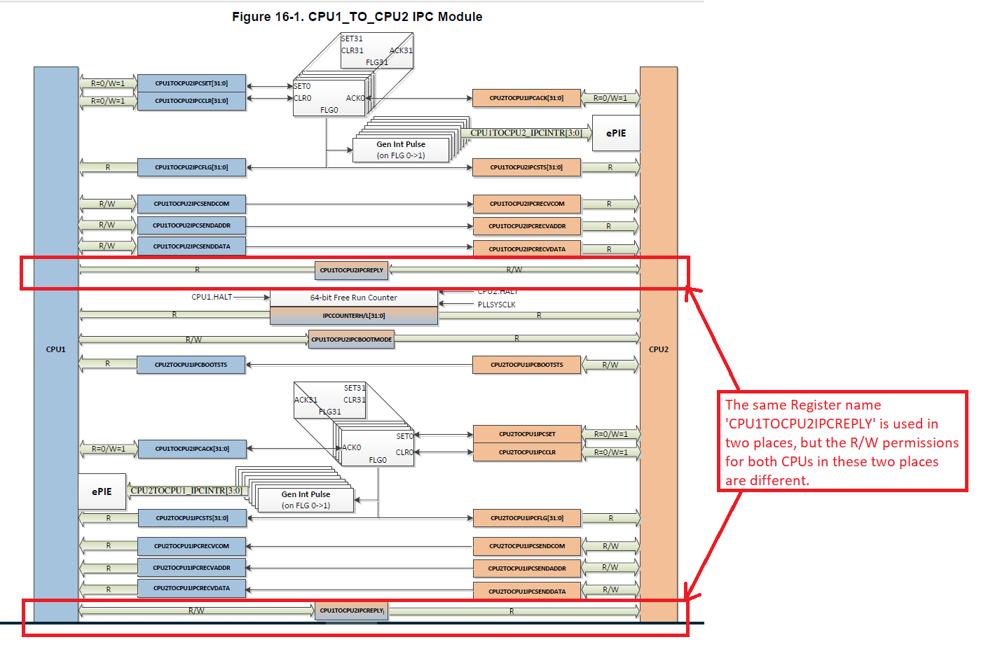
I see the same Register name 'CPU1TOCPU2IPCREPLY' is used two places the IPC module diagram as shown below:

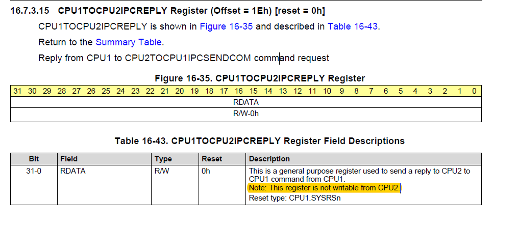
Similarly, the same register description is present for the CPU2TOCPU1IPCREPLY register in section 16.7.2.15 from CPU1TOCPU2_IPC_REGS_CPU1VIEW registers and in section 16.7.3.15 from CPU1TOCPU2_IPC_REGS_CPU2VIEW registers. It is mentioned CPU2 does not have write access in both places as below:


Please correct the inconsistency in the document and update the correct information in this thread.

Best Regards

Amulrass V

  • Hi Amulrass,

    You are right. There is a typo on the Figure 16-1 in the name of register which has read (R) access  from CPU1 and read/write(R/W) access from CPU2. It should be named "CPU2TOCPU1IPCREPLY" but other details are correct. We'll correct the name in next TRM release.

    CPU2 does not have write access to CPU1TOCPU2IPCREPLY, so info in section 16.7.2.15 and section 16.7.3.15 is correct.

    Thank you for your feedback.

    Regards,

    Vivek Singh

  • Hello Vivek,

    Yes. There is typo error only in the Figure 16-1.

    I didn't see that CPU2TOCPU1IPCREPLY register is already present in TRM for both CPU1TOCPU2_IPC_REGS_CPU1VIEW registers and CPU1TOCPU2_IPC_REGS_CPU2VIEW registers with correct description. So, the info in section 16.7.2.15 and section 16.7.3.15 are correct.

    Best Regards

    Amulrass V