This thread has been locked.

If you have a related question, please click the "Ask a related question" button in the top right corner. The newly created question will be automatically linked to this question.

TMS320F280049C: Signal drops during ADC S/H operation

Part Number: TMS320F280049C
Other Parts Discussed in Thread: OPA2317, TINA-TI

Hi,

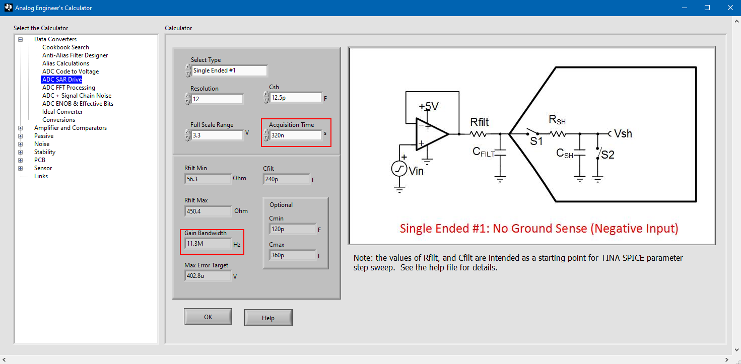
I've 2 signals (Iin_sense and Vin_sense) which have exactly the same analogue circuit driving the ADC. But Vin_sense voltage drops considerably during S/H operation as if large current is drawn while Iin_sense looks perfectly fine. Only difference I can imagine hardware wise is the different ADC input being used. A2/B6 (PIN9) is used for Vin_sense while C0 (PIN12) is being used for Iin_sense. Following are schematics and captured waveform for the Vin_sense signal. As can be seen in the waveform, there is about 160mV of voltage drop during S/H operation. On the ADC data register, I'm measuring 65mV above what I expect to read. I've set ACQPS = 31 and ADC clock equal to 100MHz. All of my other analogue signals are fine as well. It is only the Vin_sense signal which is causing the problem.

Can anyone please provide some insight? Thank you.

Regards,

Muhammad Nouman Sadiq    

  • Hi Muhammad,

    I don't think that the schematics came through on the post.  What are you driving the ADC with? What is the source impedance/capacitance and bandwidth of this circuit? How does the scope capture compare to the expected results if you simulate your circuit using the methodology in the following app. note?: https://www.ti.com/lit/an/spract6/spract6.pdf

    You can also do a sanity check of the S+H duration you've selected vs the R and C (but not op-amp driving bandwidth) on the ADC driving input using the formulas in the device TRM section "Choosing an Acquisition Window Duration".

  • Hi Devin,

    I've attached the schematics.

    What really surprise me is why voltage does NOT drop for Iin_sense but does significantly for Vin_sense during S/H. Even though analogue circuits driving them are exactly the same?InputSensors-InputSensors.pdf

  • Hi Muhammad,

    I can't explain the difference in one input seeing a drop and the other no drop; I'd expect both to see a very significant drop since there isn't much capacitance on the ADC input pin.  The only difference between these inputs are the muxed PGA functions (PGA input vs PGA output filter), but I wouldn't expect the PGA to be enabled in either case.  

    Either way, I think you are going to have some issues driving the ADC with this circuit. The OPA2317 has a bandwidth of 300kHz, but you'll need much higher bandwidth to settle the ADC input to >12 bits in 320ns.  For example, using the analog engineer's calculator (https://www.ti.com/tool/ANALOG-ENGINEER-CALC), the expected settling time for 12-bits for a 300kHz op-amp is around 10us, which is much longer than you can configure (or will likely want to configure):

    To drive the input in 320ns, you'd be looking at a drive-stage op-amp with bandwidth closer to 11MHz:

    Also note that the suggested drive-stage ADC pin capacitance is ~240pF.  This is 20 times larger than the internal ADC S+H capacitor.  This ensures that when the ADC samples by closing the S+H switch, the kick-back from the internal S+H cap is roughly less than 5% of the ADC full-scale range.  This prevents large transients on the ADC input pin which can further slow settling by forcing the op-amp to slew instead of functioning to exponentially settle a small signal. 

  • Hi Devin,

    Thank you very much. This has been very helpful. 

    I think I've figured-out why Iin_sense voltage is not dropping. I've some other signals as well which are being captured in round-robin configuration. It appears to be that S/H internal capacitance was getting pre-charged from the last conversion. 

    If I disable other conversions and just perform S/H for Iin_sense, I get a voltage drop in that signal as well. 

    I've another questions, Is the RC filter after OP-AMP and before ADC really necessary? I've seen in some TI documents in which OP-AMP is directly interfaced with the ADC.  

  • Hi Muhammad,

    Ok, that makes sense.

    You can directly drive the ADC with an op-amp, but this is generally not best practice for the reasons I mentioned above.  Adding some capacitance to the ADC input will also help you avoid false trips to your down-stream comparators from the ADC kick-back.

    Either way, I'd strongly recommend that you use the TINA-TI models provided in the app. note I linked in my initial reply to simulate at least the ADC drive-stage of your signal conditioning circuits.  You can directly measure the settling performance and kick-back magnitude this way.  You can then try out things like adding the R-C to the circuit and see the effect on the settling and kick-back.