Dear Forum,
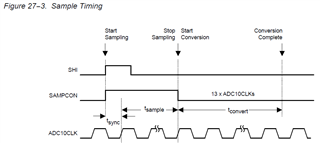
I am a little bit confused by Fig 18-3 in the MSP430F1xx manual showing how the ADC10 takes a sample.
Note, precise samping became important if higher frequency AC signals need to be digitized.
Assuming Tmer_A (TA) module OUT signal does trigg (SHI=OUT1 rise edge) the sampling (periodically).
Assuming both TA module ADC10CLK sourced also from SMCLK. TA counts the rise edge of clock.
TA OUT (and thus SHI) changes its state upon rise edge of SMCLK.
In this setup SHI trigger rising edge totally in phase with ADC10CLK thus 'tsync' ->0 according to Fig 18-3. Can it cause jitter in Sample time interval (no setup/hold time ensured to internal flip-flop) say toggles randomly between 4*Tclk / 5*Tclk?
Or certain internal mechanism allways provides the samling interval defined in the ADC10 control register (by SHTx bits)?
Thanks and regards,
Joseph