This thread has been locked.
If you have a related question, please click the "Ask a related question" button in the top right corner. The newly created question will be automatically linked to this question.
Hello, I've been trying to implement an analogue dual axis joystick using the ADC module for the MSP430FR4133, I've begun by just attaching two potentiometers to test. I've followed the example code from the slac625h library "msp430fr413x_adc10_10.c" example. Only thing I've changed is changing from 8-bit conversion to 10-bit conversion and of int format, ADCSREF_0 to AVCC,AVSS.
Code:
#include <msp430.h> unsigned int ADC_Result[3]; // 8-bit ADC conversion result array unsigned int i; int main(void) { WDTCTL = WDTPW | WDTHOLD; // Stop WDT // Configure ADC A0~2 pins SYSCFG2 |= ADCPCTL0 | ADCPCTL1 | ADCPCTL2; // Disable the GPIO power-on default high-impedance mode to activate // previously configured port settings PM5CTL0 &= ~LOCKLPM5; // Configure ADC ADCCTL0 |= ADCSHT_2 | ADCON; // 16ADCclks, ADC ON ADCCTL1 |= ADCSHP | ADCSSEL_1 | ADCSHS_2 | ADCCONSEQ_3; // ADC clock MODCLK, sampling timer, TA1.1B trig.,repeat sequence ADCCTL2 |= ADCRES; // 10-bit conversion results ADCMCTL0 |= ADCINCH_2 | ADCSREF_0; // A0~2(EoS); Vref=Vcc ADCIE |= ADCIE0; // Enable ADC conv complete interrupt // Configure reference PMMCTL0_H = PMMPW_H; // Unlock the PMM registers PMMCTL2 |= INTREFEN; // Enable internal reference __delay_cycles(400); // Delay for reference settling __no_operation(); // Configure TA1.1B as ADC trigger signal // Note: The TA1.1B is configured for 200us 50% PWM, which will trigger ADC // sample-and-conversion every 200us. The period of TA1.1B trigger event // should be more than the time period taken for ADC sample-and-conversion // and ADC interrupt service routine of each channel, which is about 57us in this code TA1CCR0 = 200-1; // PWM Period, 200us TA1CCTL1 = OUTMOD_7; // CCR1 reset/set TA1CCR1 = 100; // CCR1 PWM duty cycle, 50% TA1CTL = TASSEL__SMCLK | MC__UP | TACLR; // SMCLK, up mode, clear TAR while(1) { i = 2; ADCCTL0 |= ADCENC; // Enable ADC TA1CTL |= TACLR; // Clear TAR to start the ADC sample-and-conversion __bis_SR_register(LPM0_bits | GIE); // Enter LPM0 w/ interrupts __no_operation(); // Only for debugger } } // ADC interrupt service routine #if defined(__TI_COMPILER_VERSION__) || defined(__IAR_SYSTEMS_ICC__) #pragma vector=ADC_VECTOR __interrupt void ADC_ISR(void) #elif defined(__GNUC__) void __attribute__ ((interrupt(ADC_VECTOR))) ADC_ISR (void) #else #error Compiler not supported! #endif { switch(__even_in_range(ADCIV,ADCIV_ADCIFG)) { case ADCIV_NONE: break; case ADCIV_ADCOVIFG: break; case ADCIV_ADCTOVIFG: break; case ADCIV_ADCHIIFG: break; case ADCIV_ADCLOIFG: break; case ADCIV_ADCINIFG: break; case ADCIV_ADCIFG: ADC_Result[i] = ADCMEM0; if(i == 0) { __no_operation(); // Only for debugger i = 2; } else { i--; } break; default: break; } }
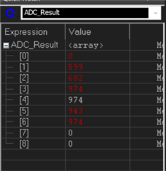
I've been at this for the past couple of days but I can't quite seem to wrap my head around as to why the A0 reading seems to not be reading from the potentiometer correctly. But A1 reading seems to be perfect. A2 is just the P1.2 button (works fine; displays 0 when pressed).
Here is my wiring diagram:
(Apologies for the poor diagram)
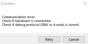
I've also noticed another anomolie, if I trim the pot too far (10k) on A0, IAR gives me the following error and my program just hangs during debugging:
I've tried using alternative pots but same error.
Your much is very much appreciated!
Aaron
What platform are you using? If you're using the Launchpad, did you disconnect LED1 from P1.0?
Hi, thanks for responding back, yes I am using the MSP430FR4133 launchpad, by disconnecting LED1 I presume the jumper connector (JP1) next to it, I've just removed it there and still observing same behaviour.
What results are you getting for A0? I.e., what is your test sequence?
------------------
> ADCCTL1 |= ADCSHP | ADCSSEL_1 | ADCSHS_2 | ADCCONSEQ_3; // ADC clock MODCLK, sampling timer, TA1.1B trig.,repeat sequence
ADCSSEL=1 sets the ADC clock to ACLK (32kHz), so a conversion takes (16+13)*30.5us=885us, but the trigger goes off every 200us, so you'll get trigger overflows (ADCTOV). The User Guide doesn't really describe what happens in this case. I suggest you change this back to
> ADCCTL1 |= ADCSHP | ADCSSEL_0 | ADCSHS_2 | ADCCONSEQ_3; // ADC clock MODCLK, sampling timer, TA1.1B trig.,repeat sequence
[I'm comparing your code to this:
https://dev.ti.com/tirex/explore/node?node=A__AE84sEwNMQaWLxkyStgOPg__msp430ware__IOGqZri__LATEST
]
Sorry, I should have posted my results, here they are:
A1 is working fine (pot trimmed all the way to 0), A0 is the one having issues, A2 is the button (wil hover around this value unless pressed in which case will turn 0).
After turning A1 pot to max, A0 to max before prescribed error occurs and A2 button pressed down:
I've also changed it back to MODCLK as per your suggestion. So it seems as though A2 and A1 is reading fine.
I'm not a EE, but I suggest you not set the pot to 0 Ohms, since that looks like a short (which could cause the board, and the debugger, to malfunction). The Ax pins are mostly high-impedance, but GND is not. I think the last time I used a pot I made a resistor divider out of it for just this reason.
More generally, one hazard with a pot is that it's easy to end up with a source with fairly high impedance, which will require a longer Sample/Hold time to charge the ADC capacitor. UG (SLAU445I) Sec 21.2.5.3 gives a formula, but a quick experiment would be to set ADCSHT very high and see if the symptom changes. (This will also probably bump up against your timer-trigger period, so you might want to increase that as well.)
Another quick experiment would be to set ADCINCH=0, to see if A0 works better in isolation.
I just noticed that P1.0 is also connected to the backchannel UART via J101 ("bridge jumper block"). I suggest you remove the TXD and RXD jumpers; I'm a little surprised that P1.1 (RXD) isn't being affected.
I'm not a EE, but I suggest you not set the pot to 0 Ohms, since that looks like a short
The symbol used hides the details so this may not be the case. With the center wiper connected only to the ADC input, then no. But you will end up with a low impedance connection to ground and Vcc when at either end of travel. Which could cause trouble. Depending. (If the pin is used as an output, TXD for example, that would be a problem.) I prefer a symbol that makes explicit the three terminals and how they are connected.
One use of a variable resistor connects the center wiper to one of the other terminals. Not useful here since the wiper voltage is constant. But you will create a short between the two non wiper terminals when set to minimum resistance.
Hi Aaron,
I think David and Bruce are on the right track here, try again with your UART jumpers pulled and please report back.
Best Regards,
Brandon
Hi, that seemed to have fixed it, although my application requires TXD and RXD jumpers to be activated for UART transmission so I tried to now use A8 (P8.0) and A5 (P1.5) (the only other available pins) but it seems to just be reading random noise:
#include <msp430.h> unsigned int ADC_Result[3]; // 8-bit ADC conversion result array unsigned int i; int main(void) { WDTCTL = WDTPW | WDTHOLD; // Stop WDT // Configure ADC A0~8 pins SYSCFG2 |= ADCPCTL0 | ADCPCTL5 | ADCPCTL8; // Disable the GPIO power-on default high-impedance mode to activate // previously configured port settings PM5CTL0 &= ~LOCKLPM5; // Configure ADC ADCCTL0 |= ADCSHT_2 | ADCON; // 16ADCclks, ADC ON ADCCTL1 |= ADCSHP | ADCSHS_2 | ADCCONSEQ_3; // ADC clock MODCLK, sampling timer, TA1.1B trig.,repeat sequence ADCCTL2 |= ADCRES; // 10-bit conversion results ADCMCTL0 |= ADCINCH_8 | ADCSREF_0; // A0~2(EoS); Vref=Vcc ADCIE |= ADCIE0; // Enable ADC conv complete interrupt // Configure reference PMMCTL0_H = PMMPW_H; // Unlock the PMM registers PMMCTL2 |= INTREFEN; // Enable internal reference __delay_cycles(400); // Delay for reference settling __no_operation(); // Configure TA1.1B as ADC trigger signal // Note: The TA1.1B is configured for 200us 50% PWM, which will trigger ADC // sample-and-conversion every 200us. The period of TA1.1B trigger event // should be more than the time period taken for ADC sample-and-conversion // and ADC interrupt service routine of each channel, which is about 57us in this code TA1CCR0 = 200-1; // PWM Period, 200us TA1CCTL1 = OUTMOD_7; // CCR1 reset/set TA1CCR1 = 100; // CCR1 PWM duty cycle, 50% TA1CTL = TASSEL__SMCLK | MC__UP | TACLR; // SMCLK, up mode, clear TAR while(1) { i = 2; ADCCTL0 |= ADCENC; // Enable ADC TA1CTL |= TACLR; // Clear TAR to start the ADC sample-and-conversion __bis_SR_register(LPM0_bits | GIE); // Enter LPM0 w/ interrupts __no_operation(); // Only for debugger } } // ADC interrupt service routine #if defined(__TI_COMPILER_VERSION__) || defined(__IAR_SYSTEMS_ICC__) #pragma vector=ADC_VECTOR __interrupt void ADC_ISR(void) #elif defined(__GNUC__) void __attribute__ ((interrupt(ADC_VECTOR))) ADC_ISR (void) #else #error Compiler not supported! #endif { switch(__even_in_range(ADCIV,ADCIV_ADCIFG)) { case ADCIV_NONE: break; case ADCIV_ADCOVIFG: break; case ADCIV_ADCTOVIFG: break; case ADCIV_ADCHIIFG: break; case ADCIV_ADCLOIFG: break; case ADCIV_ADCINIFG: break; case ADCIV_ADCIFG: ADC_Result[i] = ADCMEM0; if(i == 0) { __no_operation(); // Only for debugger i = 2; } else { i--; } break; default: break; } }
Thanks so much for you help so far
With CONSEQ=3 (or =1) the ADC samples from ADCINCH down to A0 [Ref UG (SLAU445I) Sec 21.2.7.4]., so you're getting 9 samples per round but (I'm guessing) you're stopping every 3. I suggest you expand your array to [9].
Sampling channels you haven't enabled is a bit of a waste, but doesn't normally cause trouble.
With that in mind now, heres what I am getting:
I should only see a reading in [8] and [5]. 0 elsewhere. I currently have some pins connected externally, will this impact the reading?
/* --COPYRIGHT--,BSD_EX * Copyright (c) 2014, Texas Instruments Incorporated * All rights reserved. * * Redistribution and use in source and binary forms, with or without * modification, are permitted provided that the following conditions * are met: * * * Redistributions of source code must retain the above copyright * notice, this list of conditions and the following disclaimer. * * * Redistributions in binary form must reproduce the above copyright * notice, this list of conditions and the following disclaimer in the * documentation and/or other materials provided with the distribution. * * * Neither the name of Texas Instruments Incorporated nor the names of * its contributors may be used to endorse or promote products derived * from this software without specific prior written permission. * * THIS SOFTWARE IS PROVIDED BY THE COPYRIGHT HOLDERS AND CONTRIBUTORS "AS IS" * AND ANY EXPRESS OR IMPLIED WARRANTIES, INCLUDING, BUT NOT LIMITED TO, * THE IMPLIED WARRANTIES OF MERCHANTABILITY AND FITNESS FOR A PARTICULAR * PURPOSE ARE DISCLAIMED. IN NO EVENT SHALL THE COPYRIGHT OWNER OR * CONTRIBUTORS BE LIABLE FOR ANY DIRECT, INDIRECT, INCIDENTAL, SPECIAL, * EXEMPLARY, OR CONSEQUENTIAL DAMAGES (INCLUDING, BUT NOT LIMITED TO, * PROCUREMENT OF SUBSTITUTE GOODS OR SERVICES; LOSS OF USE, DATA, OR PROFITS; * OR BUSINESS INTERRUPTION) HOWEVER CAUSED AND ON ANY THEORY OF LIABILITY, * WHETHER IN CONTRACT, STRICT LIABILITY, OR TORT (INCLUDING NEGLIGENCE OR * OTHERWISE) ARISING IN ANY WAY OUT OF THE USE OF THIS SOFTWARE, * EVEN IF ADVISED OF THE POSSIBILITY OF SUCH DAMAGE. * ******************************************************************************* * * MSP430 CODE EXAMPLE DISCLAIMER * * MSP430 code examples are self-contained low-level programs that typically * demonstrate a single peripheral function or device feature in a highly * concise manner. For this the code may rely on the device's power-on default * register values and settings such as the clock configuration and care must * be taken when combining code from several examples to avoid potential side * effects. Also see www.ti.com/grace for a GUI- and www.ti.com/msp430ware * for an API functional library-approach to peripheral configuration. * * --/COPYRIGHT--*/ //****************************************************************************** // MSP430FR413x Demo - ADC, Sample A2/A1/A0, internal 1.5V Ref. // // Description: This example works on Repeat-sequence-of-channels Mode // with TA1.1B as the trigger signal. // A2/A1/A0 is sampled 16ADCclks with reference to 1.5V. // Internal oscillator times sample (16x) and conversion(13x). // Inside ADC_ISR A2/A1/A0 sample value put into array ADC_Result[3]. // ACLK = default REFO ~32768Hz, MCLK = SMCLK = default DCODIV ~1MHz. // // Note: The TA1.1B is configured for 200us 50% PWM, which will trigger ADC // sample-and-conversion every 200us. The period of TA1.1B trigger event // should be more than the time period taken for ADC sample-and-conversion // and ADC interrupt service routine of each channel, which is about 57us in this code // // // MSP430FR4133 // ----------------- // /|\| | // | | | // --|RST | // | | // >---|P1.2/A2 | // >---|P1.1/A1 | // >---|P1.0/A0 | // // // Wei Zhao // Texas Instruments Inc. // July 2018 // Built with IAR Embedded Workbench v7.11 & Code Composer Studio v7.4 //****************************************************************************** #include <msp430.h> unsigned int ADC_Result[9]; // 8-bit ADC conversion result array unsigned int i; int main(void) { WDTCTL = WDTPW | WDTHOLD; // Stop WDT // Configure ADC A0~2 pins SYSCFG2 |= ADCPCTL0 | ADCPCTL5 | ADCPCTL8; // Disable the GPIO power-on default high-impedance mode to activate // previously configured port settings PM5CTL0 &= ~LOCKLPM5; // Configure ADC ADCCTL0 |= ADCSHT_2 | ADCON; // 16ADCclks, ADC ON ADCCTL1 |= ADCSHP | ADCSHS_2 | ADCCONSEQ_3; // ADC clock MODCLK, sampling timer, TA1.1B trig.,repeat sequence ADCCTL2 |= ADCRES; // 10-bit conversion results ADCMCTL0 |= ADCINCH_8 | ADCSREF_0; // A0~2(EoS); Vref=1.5V ADCIE |= ADCIE0; // Enable ADC conv complete interrupt // Configure reference PMMCTL0_H = PMMPW_H; // Unlock the PMM registers PMMCTL2 |= INTREFEN; // Enable internal reference __delay_cycles(400); // Delay for reference settling __no_operation(); // Configure TA1.1B as ADC trigger signal // Note: The TA1.1B is configured for 200us 50% PWM, which will trigger ADC // sample-and-conversion every 200us. The period of TA1.1B trigger event // should be more than the time period taken for ADC sample-and-conversion // and ADC interrupt service routine of each channel, which is about 57us in this code TA1CCR0 = 200-1; // PWM Period, 200us TA1CCTL1 = OUTMOD_7; // CCR1 reset/set TA1CCR1 = 100; // CCR1 PWM duty cycle, 50% TA1CTL = TASSEL__SMCLK | MC__UP | TACLR; // SMCLK, up mode, clear TAR while(1) { i = 9; ADCCTL0 |= ADCENC; // Enable ADC TA1CTL |= TACLR; // Clear TAR to start the ADC sample-and-conversion __bis_SR_register(LPM0_bits | GIE); // Enter LPM0 w/ interrupts __no_operation(); // Only for debugger } } // ADC interrupt service routine #if defined(__TI_COMPILER_VERSION__) || defined(__IAR_SYSTEMS_ICC__) #pragma vector=ADC_VECTOR __interrupt void ADC_ISR(void) #elif defined(__GNUC__) void __attribute__ ((interrupt(ADC_VECTOR))) ADC_ISR (void) #else #error Compiler not supported! #endif { switch(__even_in_range(ADCIV,ADCIV_ADCIFG)) { case ADCIV_NONE: break; case ADCIV_ADCOVIFG: break; case ADCIV_ADCTOVIFG: break; case ADCIV_ADCHIIFG: break; case ADCIV_ADCLOIFG: break; case ADCIV_ADCINIFG: break; case ADCIV_ADCIFG: ADC_Result[i] = ADCMEM0; if(i == 0) { __no_operation(); // Only for debugger i = 9; } else { i--; } break; default: break; } }
Thanks
> i = 9;
This should be "i = 8;". Besides the array-bounds thing, this will cause the array entries to cycle off-by-1.
------------
The readings for the "uninteresting" An channels (A1-A4,A6-A7) won't (in general) be =0, they'll be whatever the respective pin says. E.g., A1=P1.1 (RXD) will read close to 1023 since the eZ-FET (backchannel UART) is driving it high.
**Attention** This is a public forum