This thread has been locked.

If you have a related question, please click the "Ask a related question" button in the top right corner. The newly created question will be automatically linked to this question.

MSP430FR5043: Register settings question for SDHS ADC in "raw" register mode - no bias

Part Number: MSP430FR5043

Hello everyone,

We are looking for some sample code and additional information on how to acquire raw ADC data from the SDHS system of the MSP430FR5043.

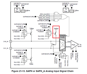
i.e. We would like to bypass the USS system control, and simply acquire samples from CH0_IN without any bias directly by the ADC at 8Msps

I understand this is possible in "register mode", but it is unclear how to disable the Rx and Tx Bias on the input, and then what the actual input voltage input range will be.

If the bias was disabled, then would the input voltage range be 0 to 1V?

Can CH0_IN be driven directly by an opamp?

Does the CH0_IN always need to be AC coupled due to a limitation in the input structure?

Thanks much for your help and advice.

  • Thanks much Johnson - this is very helpful.

    The other issue is regarding the bias.

    The example code assumes a 0.9V bias.

    Is there a way to disable the Tx and Rx bias - The diagrams in the user guide seem to indicate this is possible, but the register descriptions are unclear.

    Is AC coupling required for the PGA input?

    Do you know where the full scale voltage of 0.755V comes from? The datasheet says it should be 1.0V?

    Thanks for your help?

    Dave

  • Hi Dave,

    Is there a way to disable the Tx and Rx bias - The diagrams in the user guide seem to indicate this is possible, but the register descriptions are unclear.

    you can find more deacription in User Guide, like this figure:

    Is AC coupling required for the PGA input?

    What means that? this PGA is not support differential input.

    Do you know where the full scale voltage of 0.755V comes from? The datasheet says it should be 1.0V?

    Thanks!

    Best Regards

    Johnson

  • Thanks again for the help Johnson,

    Regarding the Rx and Tx Bias, I think I understand now that the SAPHBCTL register is the one that actually controls whether the bias is on or off. The diagram is very complex.

    For AC coupling, I was wondering if there was some limitation on the CH0_IN input pin that requires AC coupling, since I see a capacitor on the input of all the example designs. Can I assume that if both Tx and Rx bias is turned off, then AC coupling is not required?

    Lastly, regarding the input voltage range, the datasheet specifies a "max" input range of 800mV when PVCC is less than 2.5V and a "max" input range of 1000mV when PVCC is greater than 2.5V. However, I don't see the actual expected input voltage range specified anywhere, and I don't see where 0.755V comes from. Is there a way to know what the expected input voltage range will be?

    Thanks again.

    Dave

  • Hi Dave,

    We added a capacitor in USS_IN pin to avoid DC signal to PGA, then enable Bias to add a offset to avoid negative voltage. PGA input is 0~800mV.

    For AC coupling, I was wondering if there was some limitation on the CH0_IN input pin that requires AC coupling, since I see a capacitor on the input of all the example designs. Can I assume that if both Tx and Rx bias is turned off, then AC coupling is not required?

    Expected input is less than 800mV when PVCC=2.5V, 0.755 is juat a recommender value to keep more good performance for SDHS. We use Herbert algorithm to calculate dTOF, thus we don't need too much Vpp, 0.755 is enough.

    Lastly, regarding the input voltage range, the datasheet specifies a "max" input range of 800mV when PVCC is less than 2.5V and a "max" input range of 1000mV when PVCC is greater than 2.5V. However, I don't see the actual expected input voltage range specified anywhere, and I don't see where 0.755V comes from. Is there a way to know what the expected input voltage range will be?

    Thanks!

    Best Regards

    Johnson

**Attention** This is a public forum