This thread has been locked.

If you have a related question, please click the "Ask a related question" button in the top right corner. The newly created question will be automatically linked to this question.

MSP430FR2672: Use of conductive bridging material vs conductive ink

Part Number: MSP430FR2672

Hello,

I am working on a design with very long curved slider elements. We are having some issues with our mechanical layer-stack dramatically decreasing sensitivity. We are going through the process of optimizing the materials, thickness, and eliminating air gaps.

During this process our OEM suggested that we use conductive ink as their other customers have to improve performance. My immediate response was no. But there seems to be some conflicting information on your design guide I would like some clarification on.

In your example of a typical stack-up you indicate that the stack-up should be non conductive which makes sense. As a conductive material in the stack-up will act as a shield if grounded, or a floating unknown capacitance if left floating, and potentially something in between. See link below:

https://software-dl.ti.com/msp430/msp430_public_sw/mcu/msp430/CapTIvate_Design_Center/latest/exports/docs/users_guide/html/CapTIvate_Technology_Guide_html/markdown/ch_design_guide.html#typical-stackup

Then you mention the use a conductive foam as a bridging material just a couple sections later. I am familiar with the concept of using a conductive bridge to basically extend a single cap-touch element away from the PCBA. i.e. adding a single spring to a single button. This makes sense to me as it is just acting as an extension of a single capacitive interaction between your finger and the pad. By the same token a conductive foam would server the same purpose.

My question is that when you move to a slider, does a conductive foam laid over all 4 elements act more as a shield than a conductive extension? Would each slider element need a separate piece of foam?

https://software-dl.ti.com/msp430/msp430_public_sw/mcu/msp430/CapTIvate_Design_Center/latest/exports/docs/users_guide/html/CapTIvate_Technology_Guide_html/markdown/ch_design_guide.html#id23

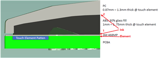
This leads me to my real question here, of will adding a conductive paint to the back side of a piece of ABS that is adhered our PCB via 3M 468MP help or hurt our touch slider?

  • 1. Can you show me how you will use the conductive ink?

    does a conductive foam laid over all 4 elements act more as a shield than a conductive extension? Would each slider element need a separate piece of foam?

    2. It will ack as a conductive extension if they are connected to the slider element one by one. If they are connected to the GND or floating, it will ack as a shield.

    3. If you use the coductive ink as the element extension, it will absolutely increase the sensivity.  

  • Hello Eason,

    1. I do not have CAD to show you what we are currently discussing with our OEM. However, I have attached a pdf showing the touch element pattern, and another pdf with the conductive ink specification. I also attached a cross section of our stack-up showing the materials used and where the conductive ink would be printed. What has been suggested to us is printing the back of the plastic overlay with this conductive ink in a pattern that exactly matches the pattern on the PCBA.

    2. Are you saying that there must be electrical connection between the conductive ink and the touch elements? i.e. cannot use solder mask on touch element and must use conductive adhesive for electrically connecting touch element to the conductive ink? Or can the conductive ink match the pattern of the touch element and be separated from the PCBA by solder mask and 3M 468MP?

    3. Do you think just adding conductive ink in the proposed location will increase sensitivity?

    D10969 conductive ink.pdfElement_1.pdfTouch Element Stackup.pdf

  • To be clarify, you can use any coducted materials as the element, like Cu or coducted ink. And then connect the element to MCU IO.

    If you want to use the coducted ink as the element, I think you should remove the element on PCB. Because you increase the area to coupling to GND, which will reduce the senvisity.

    If the ink is at 1, I think the senvity will only increase a little.


    I would suggest you refer to this doc: https://www.ti.com/lit/ug/slau857a/slau857a.pdf?ts=1695102906651&ref_url=https%253A%252F%252Fwww.ti.com%252Fproduct%252FMSP430FR2633 to have a better understand about sensivity factors.

**Attention** This is a public forum