This thread has been locked.

If you have a related question, please click the "Ask a related question" button in the top right corner. The newly created question will be automatically linked to this question.

PCB design around 32768Hz crystal?

Other Parts Discussed in Thread: MSP430F5359, MSP430G2553

Hello,

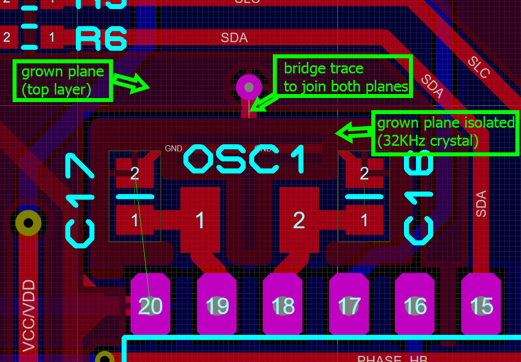
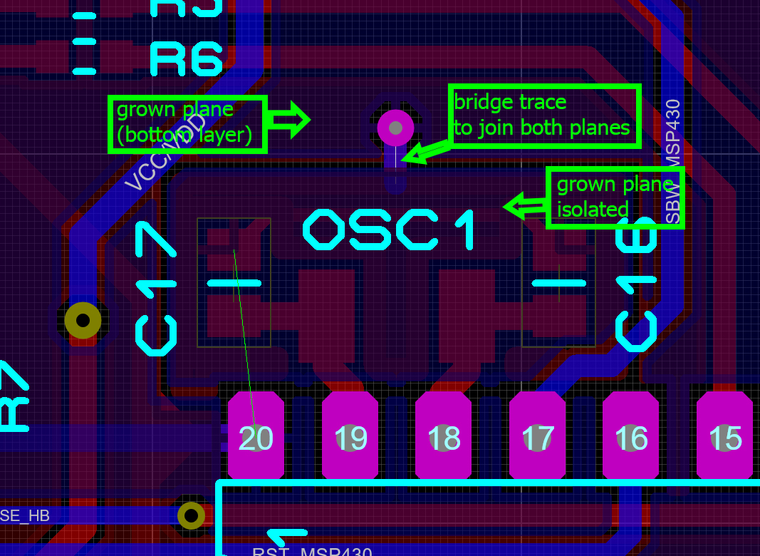
I would be grateful if someone could give me a clarification to figure 8 in SLAA322B.

http://www.ti.com/lit/an/slaa322b/slaa322b.pdf

In the right PCB layout: Is red copper top and blue copper bottom?

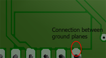
If blue is a "GND island isolated by a gap from the rest of the GND" should that GND island be connected to the rest of the GND just at AVSS1 (MSP430F5359)? 

At the moment I just have a ground plane on copper bottom which also covers the crystal area (no gap isolating the ground plane under the crystal). Is that a problem? Wouldn't a isolated ground plane produce a lot of EMI?

Best Regards

Kalle Ohlsson

  • Hi Kalle,

    Yes, the red indicated top copper and the blue indicates bottom copper.

    Having an isolated ground plane underneath the crystal is a typical "best practice" in design.  I won't say that it is required, but if you have the capability in your layout to isolate the crystal, it would be beneficial to do so.  It comes down to what kind of accuracy and precision do you need from the oscillator.  Isolating the ground plane helps to prevents ground currents from propagating underneath the crystal.  Lots of things come in to play, like the quality and size of the crystal as well as the layout.

    With regard to EMI, the plane is only "isolated" in the sense that it is connected to the rest of the ground plane at one point.  The goal here is to simply have it behave as a shield, and not as a power plane that flows ground currents.  Having the isolated plane helps you with RF susceptibility; having a ground plane in general (underneath the crystal) helps you with RF emissions.

    Are you designing a two layer board, or something larger?  You will also want to ensure that you do not run any digital signals or power signals underneath the crystal either.

    Here is another similar post that you may find interesting:

    http://e2e.ti.com/support/microcontrollers/msp430/f/166/t/118247.aspx


    Regards,
    Walter

  • Hi Walter,

    Thank you very much for your answer. We are using a 2 layer pcb and have no traces under the crystal.

    Regards

    Kalle

  • Hello! I am designing a PCB with two layers with a ground plane in each. The MSP430G2553 and 32KHz crystal are on the top layer. I have two options and I do not know which one is the best.

    1. Create an isolated ground plane in the two layers, as recommended in this document (http://www.ti.com/lit/an/slaa322b/slaa322b.pdf) and connect both by a single point through a path, for example.
    2. Create the isolated ground plane and connect it by a single point, only in the bottom layer. And in the top layer, in that area, do not have any type of plane (no copper).

    Thanks and best regards.

    Fran Martin.

  • The ground plane is only in the bottom layer. What do you intend to put into the top layer? The guard ring?
  • Sorry, my English level is very low. I have two grown planes, one in the top layer and one in the bottom layer. I think I'd better show you some photos of how I designed the 32KHz crystal PCB area.

    This is the top layer:

    This is the bottom layer:

    These are the 3D vision of the top layer and bottom respectively:

    Is this design correct?

    Thank you and greetings.

  • There should be no additional copper in the top plane. (Such long shapes can act like an antenna.)

    And you have DVSS at pin 20 right next to the XIN/XOUT pins; this is the place where you should connect the ground plane to the rest of the ground.

  • Thans Clemes. This is the design after your correction. Add the image if you can help someone.

    Best regards,


    Fran Martin.

**Attention** This is a public forum