This thread has been locked.

If you have a related question, please click the "Ask a related question" button in the top right corner. The newly created question will be automatically linked to this question.

G2553 SDA/SCL pin numbering for I2C

Other Parts Discussed in Thread: TCA8418

Hi there,

I'm a MSP noobie trying to get a TCA8418 to talk to the G2553 through I2C. I'm using the example code given by TI:

http://www.ti.com/lit/an/slaa382a/slaa382a.pdf

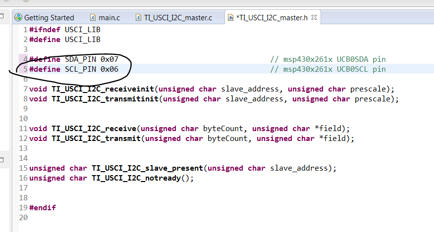
..and was told I needed to rename the SDA/SCL pins in the header file. I just wanted to confirm that I am interpreting the datasheet right when modifying the code:

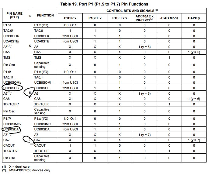
...and my resulting code:

Just wanted to rule out any mistakes. Any help would be greatly appreciated, thank you!

Best,

Oscar

  • As you can see in the source code, these two symbols are just used to configure port 3:

      P3SEL |= SDA_PIN + SCL_PIN;                 // Assign I2C pins to USCI_B0

    On your MCU, the I²C pins are not P3.6 and P3.7.

    You have to change the source code, too.

  • Hi Oscar!

    Beside from Clemens' answer there is another general mistake in your code:

    UCB0SCL is at P1.6 and UCB0SDA is at P1.7 and in your code you write 0x06 and 0x07, but this is wrong. 0x06 means Px.1 and Px.2 (both together). 0x07 means Px.0 and Px.1 and Px.2 (again together). You want 0x40 for Px.6 and 0x80 for Px.7 - look here:

    BIT0  BIT1  BIT2  BIT3  BIT4  BIT5  BIT6  BIT7
    
    0x01  0x02  0x04  0x08  0x10  0x20  0x40  0x80

    And of course you can combine them - for Px.6 and Px.7 you do

    0x40 | 0x80 == 0xC0

    Dennis

**Attention** This is a public forum