This thread has been locked.

If you have a related question, please click the "Ask a related question" button in the top right corner. The newly created question will be automatically linked to this question.

CCS/MSP430I2041: Load Program Error CCS 6.1.3 - MSP-FET430UIF

Part Number: MSP430I2041
Other Parts Discussed in Thread: MSP-FET

Tool/software: Code Composer Studio

Hi all,

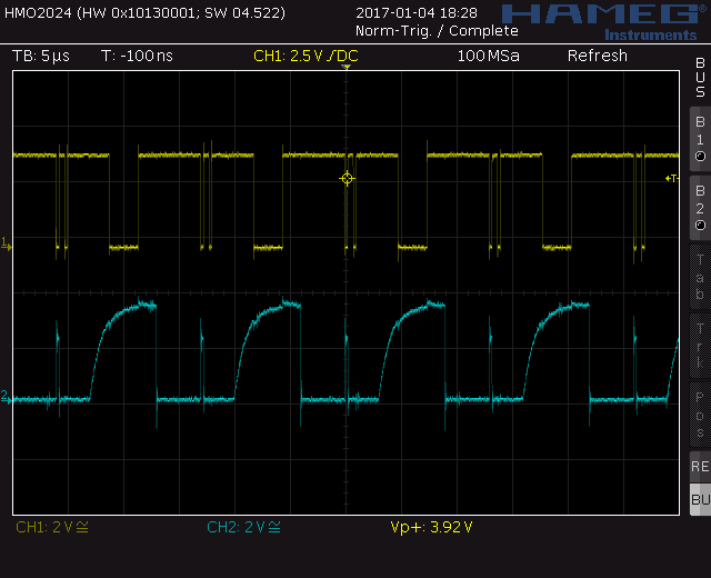
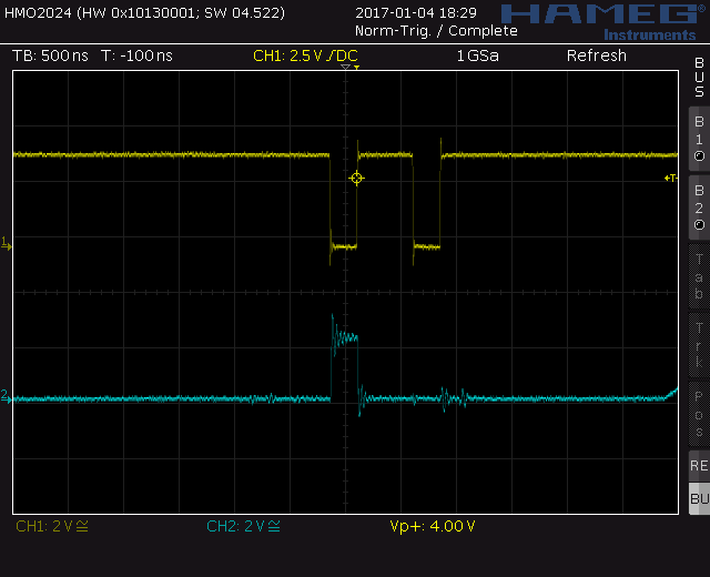
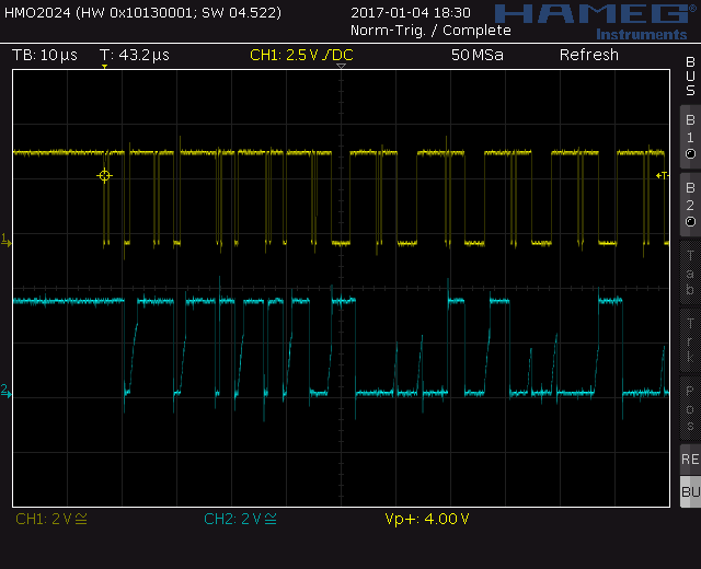
I am having problems loading the program to my target using MSP-FET430UIF . We redesign from 4 layer to 6 layers, The emulator SBW portion is the same. The 4 layer works, the 6 layer doesn't

This is the error I get: MSP430: File Loader: Verification failed: Internal error while writing 0x8000

Removing verification changes the error to: Error connecting to the target: Unknown device

Technician used Elprotronics, and lower supply to 2.0 was able to program

I appreciate any help

Marco

  • Hi Marco,
    This sounds like you're getting noise or an unclean signal on the SBW lines. Check your layers for traces that cross these lines, I've seen these interfere with various comms (I2C, SPI, etc).

    Parasitic capacitance could contribute too this as well. Can you share layouts of the 4 and 6 layer boards?
  • Cameron,

    I am trying to contact the Hardware Engineer or the layout consultant

    In the mean time, I am sending you a photo of the board, JP1 is the SBW connector, which is very close to micro pins 15 and 16.

  • Here is the partial layout and trace routing of 4-layer and 6-layer board regarding the microcontroller and JTAG connector.

    4-layer 


    6-layer


  • Cameron,

    Edward send you a partial layout in PDF

    I put together the layers stack for you. Seems we have more signals under the SBW traces as the design required in the 6 layer.  Using Elprotonic, I am able to program the flash in 6-ly if I set manually to SBW mode and the emulator supplies power and supply is 2.0V . As you can see this is not the ideal development for me, CCS does some handshake to select JTAG/SBW also this design has two processors and I am not in the point to freeze the 6-ly board yet.

    Do you have any suggestion? I will really appreciate your support

    Marco

    4-layer

    6-layer

  • Cameron,

    I forgot to indicate layer assignment, for the 6lr they are the following:

    GTO Top Overlay
    GTL Top Layer
    GP1..GP4 Internal Layers: G1 is V+,  G4 is GND
    GBL Bottom Layer
    GBO Bottom Overlay

    I turned ON only the signals ones

    Marco

  • Marco,
    I apologize for the delay, I have been out of office.
    I will email you asking for these files, as I cannot determine what each trace is from the shots provided.
    Alternatively, you could check for traces meeting any of the following criteria:
    -Any digital signals running parallel above or beneath the SBW traces.
    -Any SBW traces that are longer in the 6-ly than the 4-ly

    You could try adding a 1nF cap to the SBWTDIO line, as our spec recommends this.
  • Cameron,

    I answered the gerber files in the proper email.

    The solution may have two parts: 1) Solve the issue on the PCB layout and  2) Solve the Development process.

    We can't do much now on (1) as we have the pressure for Beta test, unless this affects EMI emissions severely (which I don't think it will), only we have to do more careful layout of that portion if we have another spin.

    For the (2), I already tried the 1 nF during the Holidays and it didn't work, seems we need to reduce cap instead increasing. What I will try is to add pull down resistors on those traces under the SBW that match the criteria you mentioned. These are almost static signals (they control analog switches), but they run long on the board and it may be reflecting the signal during the 2/4 wires JTAG detection phase of emulation tool. I will ask a technician to do that rework and will let you know. 

    Thanks 

    Marco


  • Cameron,

    We did the following experiments on the 6-layer board:
    1) To isolate the SBW layout, we lifted the pins 15 & 16 and wire direct to Flash emulator, same error
    2) We also lifted pin 13 (VCC) and wired directly to Emulator supply with 10uF and 0.01uF bypass, same error
    3) Added the 1nF to TDIO, same error
    As a side mnote, we still are able to program using Elprotonic @2V.0
    As a reference, the package marking for the Lots are:
    - 61AVLZTC for the 6-layer
    - 61CETGTC for the 4-layer

    Thanks
    Marco

  • Marco,
    I'm still looking into this.
    Please bear with me :-)
  • Marco,
    Has this device ever been loaded before? Do you see this problem with multiple devices on the 6ly board?

    How are you powering the board? If there is a separate source , you'll need to move VCC to JTAG pin 4 instead of 2.

    Is there anything else connected to the MSP that is powered by a different source?

    Regarding your wiring of the pins directly to the emulator, how long were the wires that you used?
  • Cameron,

    1) We were waiting to receive another 50 assembled boards, we asked the manufacturer to get a different lot and finally we get the boards. Lot identification s 61AVN1TC  The problem is still present. We can conclude that we have the problem in multiple devices.

    2) I am attaching a partial schematic showing the power supply.  I did the test with internal power supply, VR to JTAG pin 2 and connect the emulator to Front board, no external power supply. No success

    Also did the test with the two boards married (external supply) and connect VR to JTAG pin to 4, It also failed with the same error. The power supply for this connection is: The MAIN  board generates an ISO +5 and unregulated -5V, The VR (3.3V ) is generated from the iso +5V, the +3.3V uses a shunt Vref .

    3) No external powered devices connected to the board.

    4) For the test wiring the 4 wires, VCC, TCLK, TDIO and GND direct to emulator, I used 26AWG, 8.5" wires. 

    Thanks

    Marco

  • Marco,
    Can you try shortening your cable? Question 3 in the FAQ section of slau278 states that these cables should not exceed 8 inches. I'd shortewn well under 8 inches if you can. I think the 4-ly board was near the critical capacitance, and the 6ly pushed you over the threshold.

    Best regards
  • Cameron,

    Cable length reduced to 3", I still get the same error

    Marco


  • Hi Marco,

    I apologize this is taking so long.

    So when you say the Technician used Elprotronics, do you mean the software, hard ware or both?

    Could you try checking CCS for updates?

    Perhaps probing the lines would shed some light on this.

    In the morning I'll be reviewing this with a team mate to get you a faster resolution.

  • Another thing to try would be to slow the SBW clock. You can do this by expanding the targetConfigs folder. In the "All Connections Pane" expand all the way down to "MSP430", and you'll see box marked JTAG/SBW speed.
  • Changed SBW speed from Medium to Slow, didn't work.
  • 1) I used Elprotronic FET-Pro430 Lite software and TI MSP-FET emulator both the old, UIF as well as the new (the black one), being able to program if internal supply and 2.0V. I think people in production used the Elprotronic SW and HW same results, 2V only (I will confirm tomorrow morning)

    2)  My CCS 6.1.3 is up to date and even tried CCS 7.0.0 in another computer. No positive results

    3) These are some waveform I took for the 6 layers, on Jan/4 during the flashing session. Seems it runs some handshake but  I did some random capture, CH1 (Top) is CLK and CH2 is TDIO

    Marco

    FIG 1 ) Trigger is at TDIO which seems at HALF the voltage

    FIG 2 ) Zoom out view of FIG 1) Trigger is at TDIO which seems at HALF the voltage

    FIG 3 ) Just SBW activity 

  • Issue was taken offline. Root cause was incorrect capacitor value on VCore.

**Attention** This is a public forum