This thread has been locked.

If you have a related question, please click the "Ask a related question" button in the top right corner. The newly created question will be automatically linked to this question.

CCS/MSP430FR5994: Slave code does not enter the interrupt vector

Part Number: MSP430FR5994
Other Parts Discussed in Thread: MSP430FR5969, , MSP430WARE

Tool/software: Code Composer Studio

THIS IS MY MASTER CODE

/* --COPYRIGHT--,BSD
 * Copyright (c) 2016, Texas Instruments Incorporated
 * All rights reserved.
 *
 * Redistribution and use in source and binary forms, with or without
 * modification, are permitted provided that the following conditions
 * are met:
 *
 * *  Redistributions of source code must retain the above copyright
 *    notice, this list of conditions and the following disclaimer.
 *
 * *  Redistributions in binary form must reproduce the above copyright
 *    notice, this list of conditions and the following disclaimer in the
 *    documentation and/or other materials provided with the distribution.
 *
 * *  Neither the name of Texas Instruments Incorporated nor the names of
 *    its contributors may be used to endorse or promote products derived
 *    from this software without specific prior written permission.
 *
 * THIS SOFTWARE IS PROVIDED BY THE COPYRIGHT HOLDERS AND CONTRIBUTORS "AS IS"
 * AND ANY EXPRESS OR IMPLIED WARRANTIES, INCLUDING, BUT NOT LIMITED TO,
 * THE IMPLIED WARRANTIES OF MERCHANTABILITY AND FITNESS FOR A PARTICULAR
 * PURPOSE ARE DISCLAIMED. IN NO EVENT SHALL THE COPYRIGHT OWNER OR
 * CONTRIBUTORS BE LIABLE FOR ANY DIRECT, INDIRECT, INCIDENTAL, SPECIAL,
 * EXEMPLARY, OR CONSEQUENTIAL DAMAGES (INCLUDING, BUT NOT LIMITED TO,
 * PROCUREMENT OF SUBSTITUTE GOODS OR SERVICES; LOSS OF USE, DATA, OR PROFITS;
 * OR BUSINESS INTERRUPTION) HOWEVER CAUSED AND ON ANY THEORY OF LIABILITY,
 * WHETHER IN CONTRACT, STRICT LIABILITY, OR TORT (INCLUDING NEGLIGENCE OR
 * OTHERWISE) ARISING IN ANY WAY OUT OF THE USE OF THIS SOFTWARE,
 * EVEN IF ADVISED OF THE POSSIBILITY OF SUCH DAMAGE.
 * --/COPYRIGHT--*/
//*****************************************************************************
//! USCI_B0, SPI 3-Wire Master Incremented Data
//! This example shows how SPI master talks to SPI slave using 3-wire mode.
//! Incrementing data is sent by the master starting at 0x01. Received data is
//! expected to be same as the previous transmission.  eUSCI RX ISR is used to
//! handle communication with the CPU, normally in LPM0. If high, P1.0 indicates
//! valid data reception.  Because all execution after LPM0 is in ISRs,
//! initialization waits for DCO to stabilize against ACLK.
//! ACLK = ~32.768kHz, MCLK = SMCLK = DCO ~ 1048kHz.  BRCLK = SMCLK/2
//!
//! Use with SPI Slave Data Echo code example.  If slave is in debug mode, P1.1
//! slave reset signal conflicts with slave's JTAG; to work around, use IAR's
//! "Release JTAG on Go" on slave device.  If breakpoints are set in
//! slave RX ISR, master must stopped also to avoid overrunning slave
//! RXBUF.
//!
//!             Tested on MSP430FR5969
//!                 -----------------
//!            /|\ |                 |
//!             |  |                 |
//!    Master---+->|RST              |
//!                |                 |
//!                |             P1.6|-> Data Out (UCB0SIMO)
//!                |                 |
//!                |             P1.7|<- Data In (UCB0SOMI)
//!                |                 |
//!                |             P2.2|-> Serial Clock Out (UCB0CLK)
//!
//!
//! This example uses the following peripherals and I/O signals.  You must
//! review these and change as needed for your own board:
//! - SPI peripheral
//! - GPIO Port peripheral (for SPI pins)
//! - UCB0SIMO
//! - UCB0SOMI
//! - UCB0CLK
//!
//! This example uses the following interrupt handlers.  To use this example
//! in your own application you must add these interrupt handlers to your
//! vector table.
//! - USCI_B0_VECTOR
//!
//*****************************************************************************

#include "driverlib.h"
#include <stdio.h>

volatile uint8_t RXData = 0;
volatile uint8_t TXData = 0;
volatile uint32_t i;

void main(void)
{
    volatile uint16_t i;

    //Stop watchdog timer
    WDT_A_hold(WDT_A_BASE);

    //Set P1.0 as an output pin.
    /*

     * Select Port 1
     * Set Pin 0 as output
     */
    GPIO_setAsOutputPin(
        GPIO_PORT_P1,
        GPIO_PIN0
        );
    //Set P1.0 as Output Low.
    /*

     * Select Port 1
     * Set Pin 0 to output Low.
     */
    GPIO_setOutputLowOnPin(
        GPIO_PORT_P1,
        GPIO_PIN0
        );

    // Configure Pins for LFXIN
    //Set PJ.4 and PJ.5 as Primary Module Function Input.
    /*

     * Select Port J
     * Set Pin 4, 5 to input Primary Module Function, (LFXIN).
     */
    GPIO_setAsPeripheralModuleFunctionInputPin(
        GPIO_PORT_PJ,
        GPIO_PIN4 + GPIO_PIN5,
        GPIO_PRIMARY_MODULE_FUNCTION
        );

    //Set external frequency for XT1
    CS_setExternalClockSource(32768,0);
    //Set DCO frequency to max DCO setting
    CS_setDCOFreq(CS_DCORSEL_0,CS_DCOFSEL_3);
    //Select XT1 as the clock source for ACLK with no frequency divider
    CS_initClockSignal(CS_ACLK,CS_LFXTCLK_SELECT,CS_CLOCK_DIVIDER_1);
    //Start XT1 with no time out
    CS_turnOnLFXT(CS_LFXT_DRIVE_0);

    // Configure SPI pins
    // Configure Pins for UCB0CLK

    /*

     * Select Port 2
     * Set Pin 2 to input Secondary Module Function, (UCB0CLK).
     */
    GPIO_setAsPeripheralModuleFunctionInputPin(
        GPIO_PORT_P5,
        GPIO_PIN2,
        GPIO_SECONDARY_MODULE_FUNCTION
        );
    // Configure Pins for UCB0TXD/UCB0SIMO, UCB0RXD/UCB0SOMI
    //Set P1.6, P1.7 as Secondary Module Function Input.
    /*

     * Select Port 1
     * Set Pin 6, 7 to input Secondary Module Function, (UCB0TXD/UCB0SIMO, UCB0RXD/UCB0SOMI).
     */
    GPIO_setAsPeripheralModuleFunctionInputPin(
        GPIO_PORT_P5,
        GPIO_PIN0 + GPIO_PIN1,
        GPIO_SECONDARY_MODULE_FUNCTION
        );

    // Configure Pins for UCA1STE
           //Set P2.3 as Secondary Module Function Input.
           /*
            * Select Port 2
            * Set Pin 3 to input Secondary Module Function, (UCA1STE).
            */
       GPIO_setAsPeripheralModuleFunctionOutputPin(
               GPIO_PORT_P5,
               GPIO_PIN3,
               GPIO_SECONDARY_MODULE_FUNCTION
               );

    /*
     * Disable the GPIO power-on default high-impedance mode to activate
     * previously configured port settings
     */
    PMM_unlockLPM5();
    printf("Hello world!\n");
    //Initialize Master
    EUSCI_B_SPI_initMasterParam param = {0};
    param.selectClockSource = EUSCI_B_SPI_CLOCKSOURCE_ACLK;
    param.clockSourceFrequency = CS_getACLK();
    param.desiredSpiClock = 500000;
    param.msbFirst = EUSCI_B_SPI_MSB_FIRST;
    param.clockPhase = EUSCI_B_SPI_PHASE_DATA_CHANGED_ONFIRST_CAPTURED_ON_NEXT;
    param.clockPolarity = EUSCI_B_SPI_CLOCKPOLARITY_INACTIVITY_HIGH;
    param.spiMode = EUSCI_B_SPI_4PIN_UCxSTE_ACTIVE_LOW;
    EUSCI_B_SPI_initMaster(EUSCI_B1_BASE, &param);

    // Select 4 Pin Functionality
        EUSCI_B_SPI_select4PinFunctionality(EUSCI_B1_BASE,
        EUSCI_B_SPI_ENABLE_SIGNAL_FOR_4WIRE_SLAVE
       );

    //Enable SPI module
    EUSCI_B_SPI_enable(EUSCI_B1_BASE);

    EUSCI_B_SPI_clearInterrupt(EUSCI_B1_BASE,
                               EUSCI_B_SPI_RECEIVE_INTERRUPT
                               );

    // Enable USCI_B0 RX interrupt
    EUSCI_B_SPI_enableInterrupt(EUSCI_B1_BASE,
                                EUSCI_B_SPI_RECEIVE_INTERRUPT);

    //Wait for slave to initialize
    __delay_cycles(100);

    TXData = 0x1;                             // Holds TX data

    //USCI_B0 TX buffer ready?
    while(!EUSCI_B_SPI_getInterruptStatus(EUSCI_B1_BASE,
                                          EUSCI_B_SPI_TRANSMIT_INTERRUPT))
    {
        ;
    }

    //Transmit Data to slave
    EUSCI_B_SPI_transmitData(EUSCI_B1_BASE, TXData);

    __bis_SR_register(LPM0_bits + GIE);      // CPU off, enable interrupts
    __no_operation();                       // Remain in LPM0
}

#if defined(__TI_COMPILER_VERSION__) || defined(__IAR_SYSTEMS_ICC__)
#pragma vector=USCI_B1_VECTOR
__interrupt
#elif defined(__GNUC__)
__attribute__((interrupt(USCI_B1_VECTOR)))
#endif
void USCI_B1_ISR(void)
{
    switch(__even_in_range(UCB1IV,4))
    {
    //Vector 2 - RXIFG
    case 2:
        //USCI_B0 TX buffer ready?
        while(!EUSCI_B_SPI_getInterruptStatus(EUSCI_B1_BASE,
                                              EUSCI_B_SPI_TRANSMIT_INTERRUPT))
        {
            ;
        }

        RXData = EUSCI_B_SPI_receiveData(EUSCI_B1_BASE);
        if (RXData==TXData)
        {GPIO_toggleOutputOnPin(
                           GPIO_PORT_P1,
                           GPIO_PIN0
                           );

                       // Delay
                       for(i=10000; i>0; i--);}

        //Increment data
        TXData++;

        //Send next value
        EUSCI_B_SPI_transmitData(EUSCI_B1_BASE,
                                 TXData
                                 );


        //Delay between transmissions for slave to process information
        __delay_cycles(40);

        break;
    default: break;
    }
}

THIS IS MY SLAVE CODE:

/* --COPYRIGHT--,BSD
 * Copyright (c) 2016, Texas Instruments Incorporated
 * All rights reserved.
 *
 * Redistribution and use in source and binary forms, with or without
 * modification, are permitted provided that the following conditions
 * are met:
 *
 * *  Redistributions of source code must retain the above copyright
 *    notice, this list of conditions and the following disclaimer.
 *
 * *  Redistributions in binary form must reproduce the above copyright
 *    notice, this list of conditions and the following disclaimer in the
 *    documentation and/or other materials provided with the distribution.
 *
 * *  Neither the name of Texas Instruments Incorporated nor the names of
 *    its contributors may be used to endorse or promote products derived
 *    from this software without specific prior written permission.
 *
 * THIS SOFTWARE IS PROVIDED BY THE COPYRIGHT HOLDERS AND CONTRIBUTORS "AS IS"
 * AND ANY EXPRESS OR IMPLIED WARRANTIES, INCLUDING, BUT NOT LIMITED TO,
 * THE IMPLIED WARRANTIES OF MERCHANTABILITY AND FITNESS FOR A PARTICULAR
 * PURPOSE ARE DISCLAIMED. IN NO EVENT SHALL THE COPYRIGHT OWNER OR
 * CONTRIBUTORS BE LIABLE FOR ANY DIRECT, INDIRECT, INCIDENTAL, SPECIAL,
 * EXEMPLARY, OR CONSEQUENTIAL DAMAGES (INCLUDING, BUT NOT LIMITED TO,
 * PROCUREMENT OF SUBSTITUTE GOODS OR SERVICES; LOSS OF USE, DATA, OR PROFITS;
 * OR BUSINESS INTERRUPTION) HOWEVER CAUSED AND ON ANY THEORY OF LIABILITY,
 * WHETHER IN CONTRACT, STRICT LIABILITY, OR TORT (INCLUDING NEGLIGENCE OR
 * OTHERWISE) ARISING IN ANY WAY OUT OF THE USE OF THIS SOFTWARE,
 * EVEN IF ADVISED OF THE POSSIBILITY OF SUCH DAMAGE.
 * --/COPYRIGHT--*/
//*****************************************************************************
//!   SPI slave talks to SPI master using 3-wire mode. Data is received
//!   from master and data from slave is then transmitted back to master.
//!   USCI RX ISR is used to handle communication, CPU normally in LPM4.
//!   Prior to initial data exchange, master pulses slaves RST for complete
//!   reset.
//!
//!   Use with eusci_spi_ex1_master code example.  If the slave is in
//!   debug mode, the reset signal from the master will conflict with slave's
//!   JTAG; to work around, use IAR's "Release JTAG on Go" on slave device.  If
//!   breakpoints are set in slave RX ISR, master must stopped also to avoid
//!   overrunning slave RXBUF.
//!
//!              Tesed on MSP430FR5969
//!                 -----------------
//!            /|\ |                 |
//!             |  |                 |
//!    Master---+->|RST              |
//!                |                 |
//!                |             P1.6|-> Data Out (UCB0SIMO)
//!                |                 |
//!                |             P1.7|<- Data In (UCB0SOMI)
//!                |                 |
//!                |             P2.2|<- Serial Clock Out (UCB0CLK)
//!
//! This example uses the following peripherals and I/O signals.  You must
//! review these and change as needed for your own board:
//! - SPI peripheral
//! - GPIO Port peripheral (for SPI pins)
//! - UCB0SIMO
//! - UCB0SOMI
//! - UCB0CLK
//!
//! This example uses the following interrupt handlers.  To use this example
//! in your own application you must add these interrupt handlers to your
//! vector table.
//! - USCI_B0_VECTOR
//!
//
//*****************************************************************************

#include "driverlib.h"
#include <stdio.h>

volatile uint8_t transmitData = 0x01, receiveData = 0x00;
volatile uint32_t i;

void main(void)
{
    //Stop watchdog timer
    WDT_A_hold(WDT_A_BASE);

    // Configure Pins for LFXIN
    //Set PJ.4 and PJ.5 as Primary Module Function Input.
    /*
      */
    GPIO_setAsOutputPin(
        GPIO_PORT_P1,
        GPIO_PIN0
        );

    GPIO_setOutputLowOnPin(
            GPIO_PORT_P1,
            GPIO_PIN0
            );

    //
    /* Select Port J
     * Set Pin 4, 5 to input Primary Module Function, (LFXIN).
     */
    GPIO_setAsPeripheralModuleFunctionInputPin(
        GPIO_PORT_PJ,
        GPIO_PIN4 + GPIO_PIN5,
        GPIO_PRIMARY_MODULE_FUNCTION
        );

    // Configure SPI pins
    // Configure Pins for UCB0CLK

    /*

     * Select Port 2
     * Set Pin 2 to input Secondary Module Function, (UCB0CLK).
     */
    GPIO_setAsPeripheralModuleFunctionInputPin(
        GPIO_PORT_P5,
        GPIO_PIN2,
        GPIO_SECONDARY_MODULE_FUNCTION
        );
    // Configure Pins for UCB0TXD/UCB0SIMO, UCB0RXD/UCB0SOMI
    //Set P2.0, P2.1 as Secondary Module Function Input.
    /*

     * Select Port 1
     * Set Pin 6, 7 to input Secondary Module Function, (UCB0TXD/UCB0SIMO, UCB0RXD/UCB0SOMI).
     */
    GPIO_setAsPeripheralModuleFunctionInputPin(
        GPIO_PORT_P5,
        GPIO_PIN0 + GPIO_PIN1,
        GPIO_SECONDARY_MODULE_FUNCTION
        );

    // Configure Pins for UCA1STE
               //Set P2.3 as Secondary Module Function Input.
               /*
                * Select Port 2
                * Set Pin 3 to input Secondary Module Function, (UCA1STE).
                */
           GPIO_setAsPeripheralModuleFunctionOutputPin(
                   GPIO_PORT_P5,
                   GPIO_PIN3,
                   GPIO_SECONDARY_MODULE_FUNCTION
                   );

    /*
     * Disable the GPIO power-on default high-impedance mode to activate
     * previously configured port settings
     */
    PMM_unlockLPM5();

    //Initialize slave to MSB first, inactive high clock polarity and 3 wire SPI
    EUSCI_B_SPI_initSlaveParam param = {0};
    param.msbFirst = EUSCI_B_SPI_MSB_FIRST;
    param.clockPhase = EUSCI_B_SPI_PHASE_DATA_CHANGED_ONFIRST_CAPTURED_ON_NEXT;
    param.clockPolarity = EUSCI_B_SPI_CLOCKPOLARITY_INACTIVITY_HIGH;
    param.spiMode = EUSCI_B_SPI_4PIN_UCxSTE_ACTIVE_LOW;
    EUSCI_B_SPI_initSlave(EUSCI_B1_BASE, &param);

    // Select 4 Pin Functionality
           EUSCI_B_SPI_select4PinFunctionality(EUSCI_B1_BASE,
           EUSCI_B_SPI_ENABLE_SIGNAL_FOR_4WIRE_SLAVE
          );


    //Enable SPI Module
    EUSCI_B_SPI_enable(EUSCI_B1_BASE);

    EUSCI_B_SPI_clearInterrupt(EUSCI_B1_BASE,
                               EUSCI_B_SPI_RECEIVE_INTERRUPT
                               );
    //Enable Receive interrupt
    EUSCI_B_SPI_enableInterrupt(EUSCI_B1_BASE,
                                EUSCI_B_SPI_RECEIVE_INTERRUPT
                                );
    printf("Hello world!\n");
    __bis_SR_register(LPM0_bits + GIE);       // Enter LPM0, enable interrupts
}

//******************************************************************************
//
//This is the USCI_B0 interrupt vector service routine.
//
//******************************************************************************
#if defined(__TI_COMPILER_VERSION__) || defined(__IAR_SYSTEMS_ICC__)
#pragma vector=USCI_B1_VECTOR
__interrupt
#elif defined(__GNUC__)
__attribute__((interrupt(USCI_B1_VECTOR)))
#endif
void USCI_B1_ISR(void)
{
    switch(__even_in_range(UCB1IV,4))
    {
    //Vector 2 - RXIFG
    case 2:
        //USCI_B0 TX buffer ready?
        while(!EUSCI_B_SPI_getInterruptStatus(EUSCI_B1_BASE,
                                              EUSCI_B_SPI_TRANSMIT_INTERRUPT
                                              ))
        {
            ;
        }

        //Transmit data to master
        EUSCI_B_SPI_transmitData(EUSCI_B1_BASE,
                                 transmitData
                                 );

        //Receive data from master
        receiveData = EUSCI_B_SPI_receiveData(EUSCI_B1_BASE);
        printf("Hello world!\n");
        if (receiveData==transmitData)
        { GPIO_toggleOutputOnPin(
                   GPIO_PORT_P1,
                   GPIO_PIN0
                   );

               // Delay
               for(i=10000; i>0; i--);}

        //Increment data to be transmitted
        transmitData++;

        break;

    default: break;
    }
}

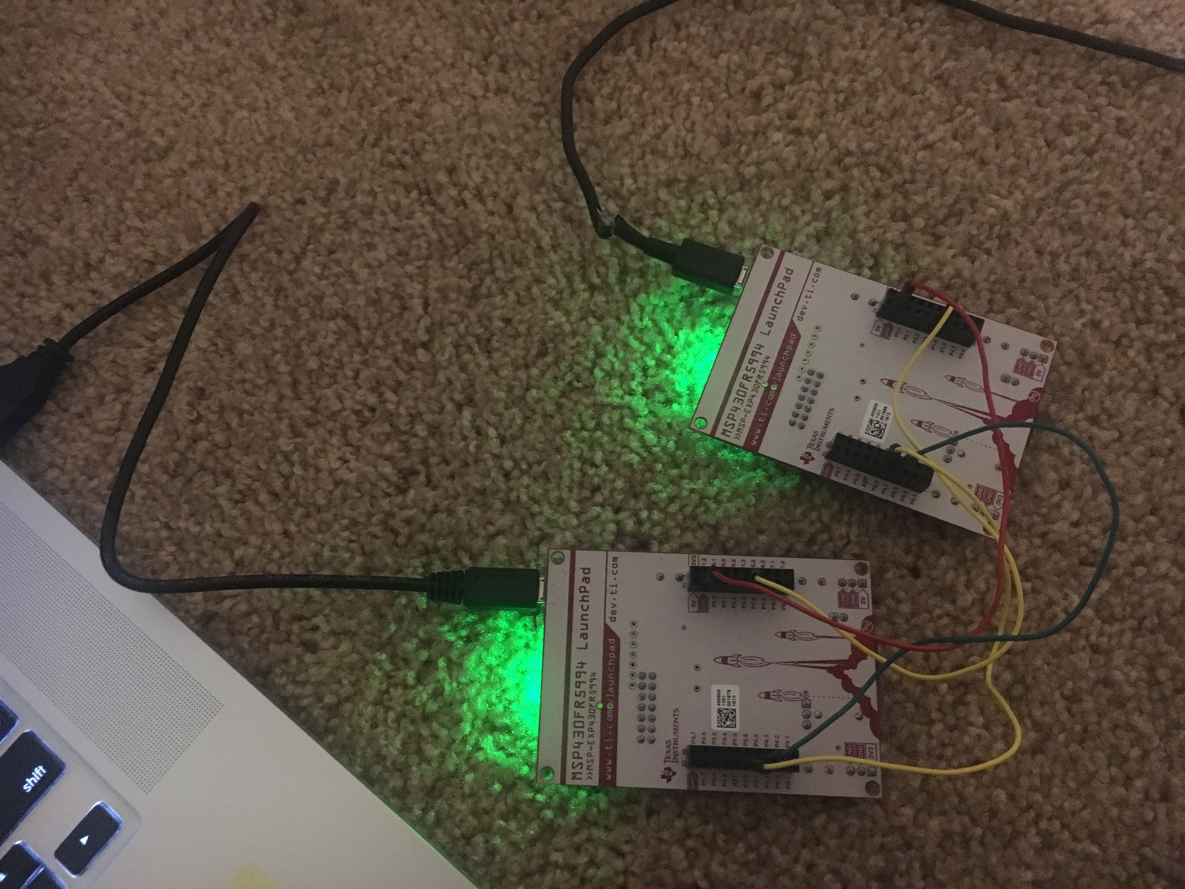
I have two MSP430FR5994 boards and I want to use SPI communication to make both boards transmit to and receive from one another. I am working with the example code provided by TI and have changed port and pin numbers in the code depending on my board.

When I run my master code on one board, the toggling of the LED happens as I increment my TXData without any connection to the slave. When I debug the slave code on the slave while it is connected to the master on which the master code is running, the slave code never enters the interrupt vector to receive the data sent by the master.

I want to use eUSCI_B1 ports for SPI so I have connected the following pins between both boards:

5V to 5V

GND to GND

P5.2 to P5.2 for UCB1CLK

P5.0 to P5.0 for UCB1SIMO

P5.1 to P5.1 for UCB1SOMI

P5.3 to P5.3 for UCB1STE


Where am I going wrong?


Thank you,

Madhu

  • Start with just the eusci_b_spi_ex1_master and eusci_b_spi_ex1_slave code, port to the FR5994, and get the simple example working before adding 4-wire mode and changing eUSCI_B peripherals. You do not need to connect the 5 V rails as they are not used (MSP operates on 3.3 V). Oscilloscope or logic analyzer screenshots would also be quite helpful. www.ti.com/.../slaa734.pdf

    Regards,
    Ryan
  • I did try both codes for eusci_b_spi_ex1_master and eusci_b_spi_ex1_slave code as well as eusci_a_spi_ex1_master and eusci_a_spi_ex1_slave code with just the 3 pin mode and it still does not work. Which is why I switched to 4 pin to see if that would make a difference. Do not have an oscilloscope so am unable to investigate this issue. I feel like something might be wrong with my connections.

    So I am using MSP430FR5994 boards and I am using pins 5.0,5.1 and 5.2 for SIMO, SOMI and CLK respectively for UCB1 and am using the appropriate functions for B SPI module in my code. Can you please let me know if I am using the right pins and my connections between the pins sounds right

    Thank you,
    Madhu
  • Your SPI connections are correct and you mentioned that the GND lines are connected but how is each LauchPad powered? The slave is most likely connected to your PC through the eZ-FET so that you can use the CCS debugger, is the master powered through its eZ-FET as well or from the slave Vcc/external power supply? If either of the latter then make sure to disconnect the eZ-FET headers, and keep in mind that 5 V is not required for this example. You can also try the FR5994 C code examples to see if these offer any different results.

    Regards,
    Ryan
  • I read somewhere that pin 5.0 of the master needs to be connected to pin 5.1 of the slave and pin 5.1 on the master needs to be connected to pin 5.0 on the slave. Is that true?

    So should I remove the connection between the 5V ports of the two boards? Should I connect the 3V ports of the two boards with a cable instead?

    So the slave is connected to my PC via a USB cable (what is an eZ-FET?) and the master is powered through an external power supply. Where are eZ-FET headers....are they in the code?

    I wasnt able to find FR5994 C code examples. Searched in a lot of places. The closest I got FR5969.

  • So now currently the ports that are connected are:

    GND to GND

    P5.2 to P5.2 for UCB1CLK

    P5.0 to P5.0 for UCB1SIMO

    P5.1 to P5.1 for UCB1SOMI

    I removed the Slave Select as I am trying the 3 pin code again

    Thank you so much for all your help! I really appreciate it!
  • The issue at hand is your PxSEL bits for P5.0 to P5.2. You are still using the GPIO_SECONDARY_MODULE_FUNCTION on the eUSCI SPI pins from when this example utilized UCB0, changing them to GPIO_PRIMARY_MODULE_FUNCTION will fix the issue. Keep the connections as shown in the images. SPI C examples (native UCB1) can be downloaded from the product's tools & software page: www.ti.com/.../slac710

    Regards,
    Ryan
  • Hi Ryan,

    Thanks a lot. Since I'm a bit new to using microcontrollers, I'm having a little trouble. Tried changing to GPIO_PRIMARY_MODULE_FUNCTION but it did not work. So I used the example code for native UCB1 and now this is currently my code:

    MASTER CODE:

    /* --COPYRIGHT--,BSD_EX
     * Copyright (c) 2015, Texas Instruments Incorporated
     * All rights reserved.
     *
     * Redistribution and use in source and binary forms, with or without
     * modification, are permitted provided that the following conditions
     * are met:
     *
     * *  Redistributions of source code must retain the above copyright
     *    notice, this list of conditions and the following disclaimer.
     *
     * *  Redistributions in binary form must reproduce the above copyright
     *    notice, this list of conditions and the following disclaimer in the
     *    documentation and/or other materials provided with the distribution.
     *
     * *  Neither the name of Texas Instruments Incorporated nor the names of
     *    its contributors may be used to endorse or promote products derived
     *    from this software without specific prior written permission.
     *
     * THIS SOFTWARE IS PROVIDED BY THE COPYRIGHT HOLDERS AND CONTRIBUTORS "AS IS"
     * AND ANY EXPRESS OR IMPLIED WARRANTIES, INCLUDING, BUT NOT LIMITED TO,
     * THE IMPLIED WARRANTIES OF MERCHANTABILITY AND FITNESS FOR A PARTICULAR
     * PURPOSE ARE DISCLAIMED. IN NO EVENT SHALL THE COPYRIGHT OWNER OR
     * CONTRIBUTORS BE LIABLE FOR ANY DIRECT, INDIRECT, INCIDENTAL, SPECIAL,
     * EXEMPLARY, OR CONSEQUENTIAL DAMAGES (INCLUDING, BUT NOT LIMITED TO,
     * PROCUREMENT OF SUBSTITUTE GOODS OR SERVICES; LOSS OF USE, DATA, OR PROFITS;
     * OR BUSINESS INTERRUPTION) HOWEVER CAUSED AND ON ANY THEORY OF LIABILITY,
     * WHETHER IN CONTRACT, STRICT LIABILITY, OR TORT (INCLUDING NEGLIGENCE OR
     * OTHERWISE) ARISING IN ANY WAY OUT OF THE USE OF THIS SOFTWARE,
     * EVEN IF ADVISED OF THE POSSIBILITY OF SUCH DAMAGE.
     *
     *******************************************************************************
     *
     *                       MSP430 CODE EXAMPLE DISCLAIMER
     *
     * MSP430 code examples are self-contained low-level programs that typically
     * demonstrate a single peripheral function or device feature in a highly
     * concise manner. For this the code may rely on the device's power-on default
     * register values and settings such as the clock configuration and care must
     * be taken when combining code from several examples to avoid potential side
     * effects. Also see www.ti.com/grace for a GUI- and www.ti.com/msp430ware
     * for an API functional library-approach to peripheral configuration.
     *
     * --/COPYRIGHT--*/
    //******************************************************************************
    //   MSP430FR5x9x Demo - eUSCI_B1, SPI 3-Wire Master Incremented Data
    //
    //   Description: SPI master talks to SPI slave using 3-wire mode. Incrementing
    //   data is sent by the master starting at 0x01. Received data is expected to
    //   be same as the previous transmission TXData = RXData-1.
    //   USCI RX ISR is used to handle communication with the CPU, normally in LPM0.
    //   ACLK = 32.768kHz, MCLK = SMCLK = DCO ~1MHz.  BRCLK = ACLK/2
    //
    //
    //                   MSP430FR5994
    //                 -----------------
    //            /|\ |              XIN|-
    //             |  |                 |  32KHz Crystal
    //             ---|RST          XOUT|-
    //                |                 |
    //                |             P5.0|-> Data Out (UCB1SIMO)
    //                |                 |
    //                |             P5.1|<- Data In (UCB1SOMI)
    //                |                 |
    //                |             P5.2|-> Serial Clock Out (UCB1CLK)
    //
    //   William Goh
    //   Texas Instruments Inc.
    //   October 2015
    //   Built with IAR Embedded Workbench V6.30 & Code Composer Studio V6.1
    //******************************************************************************
    #include <msp430.h>

    #define LED0 BIT0
    #define LED1 BIT6

    volatile unsigned char RXData = 0;
    volatile unsigned char TXData;
    volatile int i;

    int main(void)
    {
        WDTCTL = WDTPW | WDTHOLD;               // Stop watchdog timer

        // Configure GPIO
        P5SEL1 &= ~(BIT0 | BIT1 | BIT2);        // USCI_B1 SCLK, MOSI, and MISO pin
        P5SEL0 |= (BIT0 | BIT1 | BIT2);
        PJSEL0 |= BIT4 | BIT5;                  // For XT1
        P1DIR |= (LED0 + LED1); // Set P1.0 to output direction
        P1OUT &= ~(LED0 + LED1); // set P1.0 to 0 (LED OFF)
        // Disable the GPIO power-on default high-impedance mode to activate
        // previously configured port settings
        PM5CTL0 &= ~LOCKLPM5;

        // XT1 Setup
        CSCTL0_H = CSKEY_H;                     // Unlock CS registers
        CSCTL1 = DCOFSEL_0;                     // Set DCO to 1MHz
        CSCTL2 = SELA__LFXTCLK | SELS__DCOCLK | SELM__DCOCLK;
        CSCTL3 = DIVA__1 | DIVS__1 | DIVM__1;   // set all dividers
        CSCTL4 &= ~LFXTOFF;
        do
        {
            CSCTL5 &= ~LFXTOFFG;                // Clear XT1 fault flag
            SFRIFG1 &= ~OFIFG;
        } while (SFRIFG1 & OFIFG);              // Test oscillator fault flag
        CSCTL0_H = 0;                           // Lock CS registers

        // Configure USCI_B1 for SPI operation
        UCB1CTLW0 = UCSWRST;                    // **Put state machine in reset**
        UCB1CTLW0 |= UCMST | UCSYNC | UCCKPL | UCMSB; // 3-pin, 8-bit SPI master
                                                // Clock polarity high, MSB
        UCB1CTLW0 |= UCSSEL__ACLK;              // ACLK
        UCB1BRW = 0x02;                         // /2
        //UCB1MCTLW = 0;                          // No modulation
        UCB1CTLW0 &= ~UCSWRST;                  // **Initialize USCI state machine**
        UCB1IE |= UCRXIE;                       // Enable USCI_B1 RX interrupt
        TXData = 0x1;                           // Holds TX data

        while(1)
        {
            UCB1IE |= UCTXIE;
            __bis_SR_register(LPM0_bits | GIE); // CPU off, enable interrupts
    //        __delay_cycles(1000);               // Delay before next transmission
            for(i=10; i>0; i--);
            TXData=0x1;                           // Increment transmit data
        }
    }

    #if defined(__TI_COMPILER_VERSION__) || defined(__IAR_SYSTEMS_ICC__)
    #pragma vector=EUSCI_B1_VECTOR
    __interrupt void USCI_B1_ISR(void)
    #elif defined(__GNUC__)
    void __attribute__ ((interrupt(EUSCI_B1_VECTOR))) USCI_B1_ISR (void)
    #else
    #error Compiler not supported!
    #endif
    {
        switch(__even_in_range(UCB1IV, USCI_SPI_UCTXIFG))
        {
            case USCI_NONE: break;
            case USCI_SPI_UCRXIFG:
                RXData = UCB1RXBUF;
                UCB1IFG &= ~UCRXIFG;
                __bic_SR_register_on_exit(LPM0_bits); // Wake up to setup next TX
                break;
            case USCI_SPI_UCTXIFG:
                UCB1TXBUF = TXData;                   // Transmit characters
                UCB1IE &= ~UCTXIE;

                if (TXData-1==RXData)
                {P1OUT ^= (LED0 + LED1); // P1.0 = toggle
                                   // Delay
                for(i=10; i>0; i--);
                }

                break;
            default: break;
        }
    }

    SLAVE CODE:

    /* --COPYRIGHT--,BSD_EX
     * Copyright (c) 2015, Texas Instruments Incorporated
     * All rights reserved.
     *
     * Redistribution and use in source and binary forms, with or without
     * modification, are permitted provided that the following conditions
     * are met:
     *
     * *  Redistributions of source code must retain the above copyright
     *    notice, this list of conditions and the following disclaimer.
     *
     * *  Redistributions in binary form must reproduce the above copyright
     *    notice, this list of conditions and the following disclaimer in the
     *    documentation and/or other materials provided with the distribution.
     *
     * *  Neither the name of Texas Instruments Incorporated nor the names of
     *    its contributors may be used to endorse or promote products derived
     *    from this software without specific prior written permission.
     *
     * THIS SOFTWARE IS PROVIDED BY THE COPYRIGHT HOLDERS AND CONTRIBUTORS "AS IS"
     * AND ANY EXPRESS OR IMPLIED WARRANTIES, INCLUDING, BUT NOT LIMITED TO,
     * THE IMPLIED WARRANTIES OF MERCHANTABILITY AND FITNESS FOR A PARTICULAR
     * PURPOSE ARE DISCLAIMED. IN NO EVENT SHALL THE COPYRIGHT OWNER OR
     * CONTRIBUTORS BE LIABLE FOR ANY DIRECT, INDIRECT, INCIDENTAL, SPECIAL,
     * EXEMPLARY, OR CONSEQUENTIAL DAMAGES (INCLUDING, BUT NOT LIMITED TO,
     * PROCUREMENT OF SUBSTITUTE GOODS OR SERVICES; LOSS OF USE, DATA, OR PROFITS;
     * OR BUSINESS INTERRUPTION) HOWEVER CAUSED AND ON ANY THEORY OF LIABILITY,
     * WHETHER IN CONTRACT, STRICT LIABILITY, OR TORT (INCLUDING NEGLIGENCE OR
     * OTHERWISE) ARISING IN ANY WAY OUT OF THE USE OF THIS SOFTWARE,
     * EVEN IF ADVISED OF THE POSSIBILITY OF SUCH DAMAGE.
     *
     *******************************************************************************
     *
     *                       MSP430 CODE EXAMPLE DISCLAIMER
     *
     * MSP430 code examples are self-contained low-level programs that typically
     * demonstrate a single peripheral function or device feature in a highly
     * concise manner. For this the code may rely on the device's power-on default
     * register values and settings such as the clock configuration and care must
     * be taken when combining code from several examples to avoid potential side
     * effects. Also see www.ti.com/grace for a GUI- and www.ti.com/msp430ware
     * for an API functional library-approach to peripheral configuration.
     *
     * --/COPYRIGHT--*/
    //******************************************************************************
    //   MSP430FR5x9x Demo - eUSCI_B1, SPI 3-Wire Slave Data Echo
    //
    //   Description: SPI slave talks to SPI master using 3-wire mode. Data received
    //   from master is echoed back.
    //   ACLK = 32.768kHz, MCLK = SMCLK = DCO ~ 1MHz
    //   Note: Ensure slave is powered up before master to prevent delays due to
    //   slave init.
    //
    //
    //                   MSP430FR5994
    //                 -----------------
    //            /|\ |              XIN|-
    //             |  |                 |  32KHz Crystal
    //             ---|RST          XOUT|-
    //                |                 |
    //                |             P5.0|<- Data In (UCB1SIMO)
    //                |                 |
    //                |             P5.1|-> Data Out (UCB1SOMI)
    //                |                 |
    //                |             P5.2|<- Serial Clock In (UCB1CLK)
    //
    //
    //   William Goh
    //   Texas Instruments Inc.
    //   October 2015
    //   Built with IAR Embedded Workbench V6.30 & Code Composer Studio V6.1
    //******************************************************************************
    #include <msp430.h>

    #define LED0 BIT0
    #define LED1 BIT6

    volatile int i;
    volatile unsigned char rX;

    int main(void)
    {
        WDTCTL = WDTPW | WDTHOLD;               // Stop watchdog timer

        // Configure GPIO
        P5SEL1 &= ~(BIT0 | BIT1 | BIT2);        // USCI_B1 SCLK, MOSI, and MISO pin
        P5SEL0 |= (BIT0 | BIT1 | BIT2);
        PJSEL0 |= BIT4 | BIT5;

        // Disable the GPIO power-on default high-impedance mode to activate
        // previously configured port settings
        PM5CTL0 &= ~LOCKLPM5;

        // XT1 Setup
        CSCTL0_H = CSKEY_H;                     // Unlock CS registers
        CSCTL1 = DCOFSEL_0;                     // Set DCO to 1MHz
        CSCTL1 &= ~DCORSEL;
        CSCTL2 = SELA__LFXTCLK | SELS__DCOCLK | SELM__DCOCLK;
        CSCTL3 = DIVA__1 | DIVS__1 | DIVM__1;   // Set all dividers
        CSCTL4 &= ~LFXTOFF;
        do
        {
            CSCTL5 &= ~LFXTOFFG;                // Clear XT1 fault flag
            SFRIFG1 &= ~OFIFG;
        } while (SFRIFG1 & OFIFG);              // Test oscillator fault flag
        CSCTL0_H = 0;                           // Lock CS registers

        // Configure USCI_B1 for SPI operation
        UCB1CTLW0 = UCSWRST;                    // **Put state machine in reset**
        UCB1CTLW0 |= UCSYNC | UCCKPL | UCMSB;   // 3-pin, 8-bit SPI slave
                                                // Clock polarity high, MSB
        UCB1CTLW0 |= UCSSEL__SMCLK;             // ACLK
        UCB1BRW = 0x02;                         // /2
        //UCB1MCTLW = 0;                          // No modulation
        UCB1CTLW0 &= ~UCSWRST;                  // **Initialize USCI state machine**
        UCB1IE |= UCRXIE;                       // Enable USCI_B1 RX interrupt

        __bis_SR_register(LPM0_bits | GIE);     // Enter LPM0, enable interrupts
    }

    #if defined(__TI_COMPILER_VERSION__) || defined(__IAR_SYSTEMS_ICC__)
    #pragma vector=EUSCI_B1_VECTOR
    __interrupt void USCI_B1_ISR(void)
    #elif defined(__GNUC__)
    void __attribute__ ((interrupt(EUSCI_B1_VECTOR))) USCI_B1_ISR (void)
    #else
    #error Compiler not supported!
    #endif
    {
        while (!(UCB1IFG&UCTXIFG));             // USCI_B1 TX buffer ready?
        rX = UCB1RXBUF;                  // Echo received data
        if (rX==1)
        P1OUT ^= (LED0 + LED1); // P1.0 = toggle
                                       // Delay
                   // for(i=100; i>0; i--);
    }

    So when I debug the master code without the slave attached, I am able to send TXData=1 twice but not more than that as it gets stuck at __bis_SR_register(LPM0_bits | GIE); instruction (hence the LED toggles to HIGH once and then back to LOW and then nothing happens). As usual, the slave code doesnt enter the interrupt vector when master is connected and running from external power source.

    So the goal of my program is to send a 1 from the master and get it received on the slave side. If I can get this simple example to work, from there I can build something more. To achieve this, I am trying to send TXData=1 repeatedly from master side and want to receive it on the slave side so I have an if statement that if (rX==1) toggle lights.

    I believe what is happening is the send and receive are happening on the master side itself. We enter case USCI_SPI_UCTXIFG: when data is ready to transmit and then enter case USCI_SPI_UCRXIFG: to save data received into RXData and reset the interrupt flags. How can I do this receive on the slave side instead of the master side?

    Thank you,

    Madhu


  • Your project has changed from Driverlib to C code format. Since you are sampling from the echo code the master is expecting to receive an acknowledgment byte from the slave (the same value just sent) before continuing communication. Therefore the ISR on the slave side should include the following line after storing the UCB1RXBUF to rX: UCB1TXBUF = rX;

    Regards,
    Ryan

**Attention** This is a public forum