Other Parts Discussed in Thread: MSP430F6779
With Reference to the reference design:
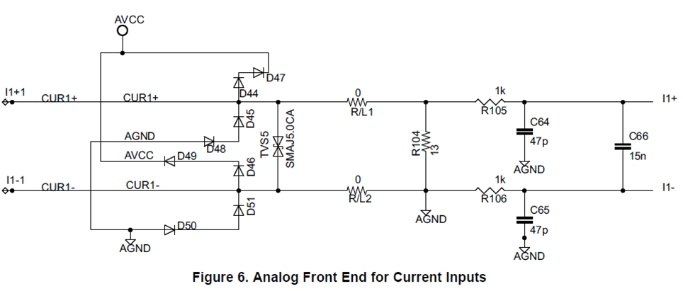
SLAA577G–January 2013–Revised August 2015
Implementation of a Three-Phase Electronic Watt-Hour
Meter Using the MSP430F677x(A)
On page 7, the analogue current front-end schematic diagram is shown (see image posed below). The SD24 ADC input has a differential input swing of +-930mV and an abs max withstand voltage of (AVss-1) for the lower limit and AVcc for the upper limit. In this reference design AVcc is 3.3V.
My Questions:
1. Diodes D44 to D51 seem to be a clamping circuit to clamp the voltage across the burden resistor (R104) to the two supply rails AGND and AVcc. Is this assumption correct?
2. If question 1 is true, why then are there two diodes placed in series? The diodes used in the design are PMLL4148 which has a maximum forward voltage of 1V. By placing two diodes in series, the voltage drop towards a supply rail is 2V. The circuit will therefore clip at +5.3V or -2V, which is way beyond the withstand limit of the SD24 input specification. Why are two diodes used in series and not just one?
3. My observation is that diodes D44 to D51 together with the TVS diode (SMAJ5.0CA) provides ESD protection (high dI/dt or dV/dt pulses) and NOT overload protection? Is this assumption correct?
4. The TVS diode (SMAJ5.0CA) clamps at 5V. It is assumed that the TVS and D44 to D51 should complement each other to provide ESD protection AND am I correct to say that the protection will only be effective if the L2 and L2 ferrite beads (omitted in the reference design) are populated?