This thread has been locked.

If you have a related question, please click the "Ask a related question" button in the top right corner. The newly created question will be automatically linked to this question.

MSP430G2553: Cannot set P2.6 to output. Want TA0.1

Part Number: MSP430G2553

Support,

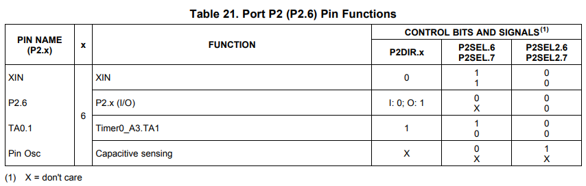
I am having difficulty setting P2.6 to output.  Specifically the TA0.1, timer output.  On the G2 LP, p2.6 is not pinned out.  But XIN/XOUT is not being used so i tacked a wire directly to the pin on the device.  I am trying to get PWM output.  Note:  It does work 100% when i use P1.6 or P1.2, per the data sheet.

WORKING: P1DIR = 0x40, P1SEL = 0x40.

NOT WORKING P2DIR = 0x40, P2SEL = 0x40

Any thoughts?

Thanks.

  • I don't have the LP schematics here, but P2.6/7 are connected to the crystal pads. Any chance there's a path to e.g. GND?
  • Hello,

    Thanks for your detailed post. When configuring P2.6 to output TA0.1, you'll need to modify five control bits: P2DIR.6, P2SEL.6 and P2SEL.7, P2SEL2.6 and P2SEL2.7. Please see Table 21 from the datasheet below. For most pins, only the PxDIR.y, PxSEL.y, and PxSEL2.y bits need to be configured, but these XIN/XOUT pins are unique.

    Regards,

    James

    MSP Customer Applications

  • James, Thank you for the response.
    I have wire tacked to pin 19, P2.6.
    I have the following setup - but still get no PWM on P2.6.

    P2DIR |= 0x40;
    P2SEL |= 0x40;
    P2SEL2 |= 0x00;
  • Why you don't use constants, for example #BIT6 instead of non-readable 0x40 value. Your last line (P2SEL2) doesn't do anything. You must clear P2SEL2 bits (with and, not or).
  • The chip boots up with P2SEL = 0xC0.  It appears from the table above that for timer output you need it to be 0x40.  But your OR instruction doesn't clear the high bit.  You also aren't changing P2SEL2, but it boots cleared, so you're probably ok there. (but still, best practice would be to clear it).

**Attention** This is a public forum