This thread has been locked.
If you have a related question, please click the "Ask a related question" button in the top right corner. The newly created question will be automatically linked to this question.
Part Number: MSP432P4111
Hi,
I have two questions.
1.
I try to set the MCU to 48MHz via the define __SYSTEM_CLOCK in the start up file "system_msp432p4111.c".
But if I upload it to the MCU an issue occured. Normally the breakpoint in main() is reached after upload. But it don't reaches this point.
The Probe in the debug view flickers between:
"Texas Instruments XDS110 USB Debug Probe/CORTEX_M4_0 (In Reset)" and
"Texas Instruments XDS110 USB Debug Probe/CORTEX_M4_0 (Running - A Reset Occured On the Target)"
and the buttons "resume" and "suspend" are disabled and grayed out.
After a while you only see this probe message:
"Texas Instruments XDS110 USB Debug Probe/CORTEX_M4_0 (In Reset)"
If I select this probe the buttons "suspend" is enabled. With pressing "suspend" you can see that it stucks in the default handler
If I terminate it I get the console message:
CORTEX_M4_0: GEL Output: Memory Map Initialization Complete
CORTEX_M4_0: GEL Output: Halting Watchdog Timer
CORTEX_M4_0: Trouble Halting Target CPU: (Error -1266 @ 0x0) Device is held in reset. Take the device out of reset, and retry the operation. (Emulation package 8.0.903.6)
If I redo the upload and terminate it I got the message:
CORTEX_M4_0: * WARNING *: The connected device is not MSP432P4111
CORTEX_M4_0: GEL Output: Memory Map Initialization Complete
CORTEX_M4_0: GEL Output: Halting Watchdog Timer
If I want to upload a working project with a __SYSTEM_CLOCK 3000000 I got this message:
CORTEX_M4_0: * WARNING *: The connected device is not MSP432P4111
CORTEX_M4_0: GEL Output: Memory Map Initialization Complete
CORTEX_M4_0: GEL Output: Halting Watchdog Timer
CORTEX_M4_0: Flash Programmer: Reading device TLV failed.
CORTEX_M4_0: Error initializing flash programming: Your XMS432P401R material is no longer supported. We recommend you moving to production-quality MSP432P401R/M silicon by ordering samples at www.ti.com/product/MSP432P401R.
CORTEX_M4_0: Loader: One or more sections of your program falls into a memory region that is not writable. These regions will not actually be written to the target. Check your linker configuration and/or memory map.
CORTEX_M4_0: File Loader: Verification failed: Values at address 0x0001FFC0 do not match Please verify target memory and memory map.
CORTEX_M4_0: GEL: File: C:\_fhnw\8_Semester\pro5E_6E\workspace_ccs\00_FFT_07_MCU4111_8kFFT_cmsis_6kSamples\Debug\00_FFT_07_MCU4111_8kFFT_cmsis_6kSamples.out: a data verification error occurred, file load failed.
Then I have to do a factory reset.
With a __SYSTEM_CLOCK of 24MHz it works.
Can anyone see the problem?
2.
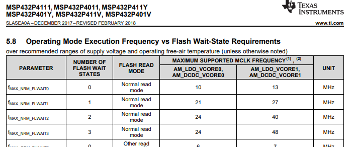
Another question is how to set flash wait states at 48MHz. From theory it should be 3 because the flash works with 16MHz. But I read the last page from "MSP432 Online Training Series - Part 4". There you can see the setup with 2 flash wait states.
Is it working with 2?
Hi Sai,
it's a long time ago, but I think it was a FFT example. This is the content of the startup file is:
/****************************************************************************** * @file system_msp432p4111.c * @brief CMSIS Cortex-M4F Device Peripheral Access Layer Source File for * MSP432P4111 * @version 3.231 * @date 01/26/18 * * @note View configuration instructions embedded in comments * ******************************************************************************/ //***************************************************************************** // // Copyright (C) 2015 - 2018 Texas Instruments Incorporated - http://www.ti.com/ // // Redistribution and use in source and binary forms, with or without // modification, are permitted provided that the following conditions // are met: // // Redistributions of source code must retain the above copyright // notice, this list of conditions and the following disclaimer. // // Redistributions in binary form must reproduce the above copyright // notice, this list of conditions and the following disclaimer in the // documentation and/or other materials provided with the // distribution. // // Neither the name of Texas Instruments Incorporated nor the names of // its contributors may be used to endorse or promote products derived // from this software without specific prior written permission. // // THIS SOFTWARE IS PROVIDED BY THE COPYRIGHT HOLDERS AND CONTRIBUTORS // "AS IS" AND ANY EXPRESS OR IMPLIED WARRANTIES, INCLUDING, BUT NOT // LIMITED TO, THE IMPLIED WARRANTIES OF MERCHANTABILITY AND FITNESS FOR // A PARTICULAR PURPOSE ARE DISCLAIMED. IN NO EVENT SHALL THE COPYRIGHT // OWNER OR CONTRIBUTORS BE LIABLE FOR ANY DIRECT, INDIRECT, INCIDENTAL, // SPECIAL, EXEMPLARY, OR CONSEQUENTIAL DAMAGES (INCLUDING, BUT NOT // LIMITED TO, PROCUREMENT OF SUBSTITUTE GOODS OR SERVICES; LOSS OF USE, // DATA, OR PROFITS; OR BUSINESS INTERRUPTION) HOWEVER CAUSED AND ON ANY // THEORY OF LIABILITY, WHETHER IN CONTRACT, STRICT LIABILITY, OR TORT // (INCLUDING NEGLIGENCE OR OTHERWISE) ARISING IN ANY WAY OUT OF THE USE // OF THIS SOFTWARE, EVEN IF ADVISED OF THE POSSIBILITY OF SUCH DAMAGE. // //***************************************************************************** #include <stdint.h> #include <ti/devices/msp432p4xx/inc/msp.h> /*--------------------- Configuration Instructions ---------------------------- 1. If you prefer to halt the Watchdog Timer, set __HALT_WDT to 1: #define __HALT_WDT 1 2. Insert your desired CPU frequency in Hz at: #define __SYSTEM_CLOCK 12000000 3. If you prefer the DC-DC power regulator (more efficient at higher frequencies), set the __REGULATOR to 1: #define __REGULATOR 1 *---------------------------------------------------------------------------*/ /*--------------------- Watchdog Timer Configuration ------------------------*/ // Halt the Watchdog Timer // <0> Do not halt the WDT // <1> Halt the WDT #define __HALT_WDT 1 /*--------------------- CPU Frequency Configuration -------------------------*/ // CPU Frequency // <1500000> 1.5 MHz // <3000000> 3 MHz // <12000000> 12 MHz // <24000000> 24 MHz // <48000000> 48 MHz #define __SYSTEM_CLOCK 48000000 // 3000000 /*--------------------- Power Regulator Configuration -----------------------*/ // Power Regulator Mode // <0> LDO // <1> DC-DC #define __REGULATOR 0 /*---------------------------------------------------------------------------- Define clocks, used for SystemCoreClockUpdate() *---------------------------------------------------------------------------*/ #define __VLOCLK 10000 #define __MODCLK 24000000 #define __LFXT 32768 #define __HFXT 48000000 /*---------------------------------------------------------------------------- Clock Variable definitions *---------------------------------------------------------------------------*/ uint32_t SystemCoreClock = __SYSTEM_CLOCK; /*!< System Clock Frequency (Core Clock)*/ /** * Update SystemCoreClock variable * * @param none * @return none * * @brief Updates the SystemCoreClock with current core Clock * retrieved from cpu registers. */ void SystemCoreClockUpdate(void) { uint32_t source = 0, divider = 0, dividerValue = 0, centeredFreq = 0, calVal = 0; int16_t dcoTune = 0; float dcoConst = 0.0; divider = (CS->CTL1 & CS_CTL1_DIVM_MASK) >> CS_CTL1_DIVM_OFS; dividerValue = 1 << divider; source = CS->CTL1 & CS_CTL1_SELM_MASK; switch(source) { case CS_CTL1_SELM__LFXTCLK: if(BITBAND_PERI(CS->IFG, CS_IFG_LFXTIFG_OFS)) { // Clear interrupt flag CS->KEY = CS_KEY_VAL; CS->CLRIFG |= CS_CLRIFG_CLR_LFXTIFG; CS->KEY = 1; if(BITBAND_PERI(CS->IFG, CS_IFG_LFXTIFG_OFS)) { if(BITBAND_PERI(CS->CLKEN, CS_CLKEN_REFOFSEL_OFS)) { SystemCoreClock = (128000 / dividerValue); } else { SystemCoreClock = (32000 / dividerValue); } } else { SystemCoreClock = __LFXT / dividerValue; } } else { SystemCoreClock = __LFXT / dividerValue; } break; case CS_CTL1_SELM__VLOCLK: SystemCoreClock = __VLOCLK / dividerValue; break; case CS_CTL1_SELM__REFOCLK: if (BITBAND_PERI(CS->CLKEN, CS_CLKEN_REFOFSEL_OFS)) { SystemCoreClock = (128000 / dividerValue); } else { SystemCoreClock = (32000 / dividerValue); } break; case CS_CTL1_SELM__DCOCLK: dcoTune = (CS->CTL0 & CS_CTL0_DCOTUNE_MASK) >> CS_CTL0_DCOTUNE_OFS; switch(CS->CTL0 & CS_CTL0_DCORSEL_MASK) { case CS_CTL0_DCORSEL_0: centeredFreq = 1500000; break; case CS_CTL0_DCORSEL_1: centeredFreq = 3000000; break; case CS_CTL0_DCORSEL_2: centeredFreq = 6000000; break; case CS_CTL0_DCORSEL_3: centeredFreq = 12000000; break; case CS_CTL0_DCORSEL_4: centeredFreq = 24000000; break; case CS_CTL0_DCORSEL_5: centeredFreq = 48000000; break; } if(dcoTune == 0) { SystemCoreClock = centeredFreq; } else { if(dcoTune & 0x1000) { dcoTune = dcoTune | 0xF000; } if (BITBAND_PERI(CS->CTL0, CS_CTL0_DCORES_OFS)) { dcoConst = *((volatile const float *) &TLV->DCOER_CONSTK_RSEL04); calVal = TLV->DCOER_FCAL_RSEL04; } /* Internal Resistor */ else { dcoConst = *((volatile const float *) &TLV->DCOIR_CONSTK_RSEL04); calVal = TLV->DCOIR_FCAL_RSEL04; } SystemCoreClock = (uint32_t) ((centeredFreq) / (1 - ((dcoConst * dcoTune) / (8 * (1 + dcoConst * (768 - calVal)))))); } break; case CS_CTL1_SELM__MODOSC: SystemCoreClock = __MODCLK / dividerValue; break; case CS_CTL1_SELM__HFXTCLK: if(BITBAND_PERI(CS->IFG, CS_IFG_HFXTIFG_OFS)) { // Clear interrupt flag CS->KEY = CS_KEY_VAL; CS->CLRIFG |= CS_CLRIFG_CLR_HFXTIFG; CS->KEY = 1; if(BITBAND_PERI(CS->IFG, CS_IFG_HFXTIFG_OFS)) { if(BITBAND_PERI(CS->CLKEN, CS_CLKEN_REFOFSEL_OFS)) { SystemCoreClock = (128000 / dividerValue); } else { SystemCoreClock = (32000 / dividerValue); } } else { SystemCoreClock = __HFXT / dividerValue; } } else { SystemCoreClock = __HFXT / dividerValue; } break; } } /** * Initialize the system * * @param none * @return none * * @brief Setup the microcontroller system. * * Performs the following initialization steps: * 1. Enables the FPU * 2. Halts the WDT if requested * 3. Enables all SRAM banks * 4. Sets up power regulator and VCORE * 5. Enable Flash wait states if needed * 6. Change MCLK to desired frequency * 7. Enable Flash read buffering */ void SystemInit(void) { // Enable FPU if used #if (__FPU_USED == 1) /* __FPU_USED is defined in core_cm4.h */ SCB->CPACR |= ((3UL << 10 * 2) | /* Set CP10 Full Access */ (3UL << 11 * 2)); /* Set CP11 Full Access */ #endif #if (__HALT_WDT == 1) WDT_A->CTL = WDT_A_CTL_PW | WDT_A_CTL_HOLD; // Halt the WDT #endif // Enable all SRAM banks while(!(SYSCTL_A->SRAM_STAT & SYSCTL_A_SRAM_STAT_BNKEN_RDY)); if (SYSCTL_A->SRAM_NUMBANKS == 4) { SYSCTL_A->SRAM_BANKEN_CTL0 = SYSCTL_A_SRAM_BANKEN_CTL0_BNK3_EN; } else { SYSCTL_A->SRAM_BANKEN_CTL0 = SYSCTL_A_SRAM_BANKEN_CTL0_BNK1_EN; } #if (__SYSTEM_CLOCK == 1500000) // 1.5 MHz // Default VCORE is LDO VCORE0 so no change necessary // Switches LDO VCORE0 to DCDC VCORE0 if requested #if __REGULATOR while((PCM->CTL1 & PCM_CTL1_PMR_BUSY)); PCM->CTL0 = PCM_CTL0_KEY_VAL | PCM_CTL0_AMR_4; while((PCM->CTL1 & PCM_CTL1_PMR_BUSY)); #endif // No flash wait states necessary // DCO = 1.5 MHz; MCLK = source CS->KEY = CS_KEY_VAL; // Unlock CS module for register access CS->CTL0 = CS_CTL0_DCORSEL_0; // Set DCO to 1.5MHz CS->CTL1 &= ~(CS_CTL1_SELM_MASK | CS_CTL1_DIVM_MASK) | CS_CTL1_SELM__DCOCLK; // Select MCLK as DCO source CS->KEY = 0; // Set Flash Bank read buffering FLCTL_A->BANK0_RDCTL &= ~(FLCTL_A_BANK0_RDCTL_BUFD | FLCTL_A_BANK0_RDCTL_BUFI); FLCTL_A->BANK1_RDCTL &= ~(FLCTL_A_BANK0_RDCTL_BUFD | FLCTL_A_BANK0_RDCTL_BUFI); #elif (__SYSTEM_CLOCK == 3000000) // 3 MHz // Default VCORE is LDO VCORE0 so no change necessary // Switches LDO VCORE0 to DCDC VCORE0 if requested #if __REGULATOR while(PCM->CTL1 & PCM_CTL1_PMR_BUSY); PCM->CTL0 = PCM_CTL0_KEY_VAL | PCM_CTL0_AMR_4; while(PCM->CTL1 & PCM_CTL1_PMR_BUSY); #endif // No flash wait states necessary // DCO = 3 MHz; MCLK = source CS->KEY = CS_KEY_VAL; // Unlock CS module for register access CS->CTL0 = CS_CTL0_DCORSEL_1; // Set DCO to 1.5MHz CS->CTL1 &= ~(CS_CTL1_SELM_MASK | CS_CTL1_DIVM_MASK) | CS_CTL1_SELM__DCOCLK; // Select MCLK as DCO source CS->KEY = 0; // Set Flash Bank read buffering FLCTL_A->BANK0_RDCTL &= ~(FLCTL_A_BANK0_RDCTL_BUFD | FLCTL_A_BANK0_RDCTL_BUFI); FLCTL_A->BANK1_RDCTL &= ~(FLCTL_A_BANK0_RDCTL_BUFD | FLCTL_A_BANK0_RDCTL_BUFI); #elif (__SYSTEM_CLOCK == 12000000) // 12 MHz // Default VCORE is LDO VCORE0 so no change necessary // Switches LDO VCORE0 to DCDC VCORE0 if requested #if __REGULATOR while((PCM->CTL1 & PCM_CTL1_PMR_BUSY)); PCM->CTL0 = PCM_CTL0_KEY_VAL | PCM_CTL0_AMR_4; while((PCM->CTL1 & PCM_CTL1_PMR_BUSY)); #endif // No flash wait states necessary // DCO = 12 MHz; MCLK = source CS->KEY = CS_KEY_VAL; // Unlock CS module for register access CS->CTL0 = CS_CTL0_DCORSEL_3; // Set DCO to 12MHz CS->CTL1 &= ~(CS_CTL1_SELM_MASK | CS_CTL1_DIVM_MASK) | CS_CTL1_SELM__DCOCLK; // Select MCLK as DCO source CS->KEY = 0; // Set Flash Bank read buffering FLCTL_A->BANK0_RDCTL &= ~(FLCTL_A_BANK0_RDCTL_BUFD | FLCTL_A_BANK0_RDCTL_BUFI); FLCTL_A->BANK1_RDCTL &= ~(FLCTL_A_BANK0_RDCTL_BUFD | FLCTL_A_BANK0_RDCTL_BUFI); #elif (__SYSTEM_CLOCK == 24000000) // 24 MHz // Default VCORE is LDO VCORE0 so no change necessary // Switches LDO VCORE0 to DCDC VCORE0 if requested #if __REGULATOR while((PCM->CTL1 & PCM_CTL1_PMR_BUSY)); PCM->CTL0 = PCM_CTL0_KEY_VAL | PCM_CTL0_AMR_4; while((PCM->CTL1 & PCM_CTL1_PMR_BUSY)); #endif // 2 flash wait state (BANK0 VCORE0 max is 24 MHz) FLCTL_A->BANK0_RDCTL &= ~FLCTL_A_BANK0_RDCTL_WAIT_MASK | FLCTL_A_BANK0_RDCTL_WAIT_2; FLCTL_A->BANK1_RDCTL &= ~FLCTL_A_BANK0_RDCTL_WAIT_MASK | FLCTL_A_BANK0_RDCTL_WAIT_2; // DCO = 24 MHz; MCLK = source CS->KEY = CS_KEY_VAL; // Unlock CS module for register access CS->CTL0 = CS_CTL0_DCORSEL_4; // Set DCO to 24MHz CS->CTL1 &= ~(CS_CTL1_SELM_MASK | CS_CTL1_DIVM_MASK) | CS_CTL1_SELM__DCOCLK; // Select MCLK as DCO source CS->KEY = 0; // Set Flash Bank read buffering FLCTL_A->BANK0_RDCTL |= (FLCTL_A_BANK0_RDCTL_BUFD | FLCTL_A_BANK0_RDCTL_BUFI); FLCTL_A->BANK1_RDCTL &= ~(FLCTL_A_BANK0_RDCTL_BUFD | FLCTL_A_BANK0_RDCTL_BUFI); #elif (__SYSTEM_CLOCK == 48000000) // 48 MHz // Switches LDO VCORE0 to LDO VCORE1; mandatory for 48 MHz setting while((PCM->CTL1 & PCM_CTL1_PMR_BUSY)); PCM->CTL0 = PCM_CTL0_KEY_VAL | PCM_CTL0_AMR_1; while((PCM->CTL1 & PCM_CTL1_PMR_BUSY)); // Switches LDO VCORE1 to DCDC VCORE1 if requested #if __REGULATOR while((PCM->CTL1 & PCM_CTL1_PMR_BUSY)); PCM->CTL0 = PCM_CTL0_KEY_VAL | PCM_CTL0_AMR_5; while((PCM->CTL1 & PCM_CTL1_PMR_BUSY)); #endif // 3 flash wait states (BANK0 VCORE1 max is 16 MHz, BANK1 VCORE1 max is 32 MHz) FLCTL_A->BANK0_RDCTL &= ~FLCTL_A_BANK0_RDCTL_WAIT_MASK | FLCTL_A_BANK0_RDCTL_WAIT_3; FLCTL_A->BANK1_RDCTL &= ~FLCTL_A_BANK1_RDCTL_WAIT_MASK | FLCTL_A_BANK1_RDCTL_WAIT_3; // DCO = 48 MHz; MCLK = source CS->KEY = CS_KEY_VAL; // Unlock CS module for register access CS->CTL0 = CS_CTL0_DCORSEL_5; // Set DCO to 48MHz CS->CTL1 &= ~(CS_CTL1_SELM_MASK | CS_CTL1_DIVM_MASK) | CS_CTL1_SELM__DCOCLK; // Select MCLK as DCO source CS->KEY = 0; // Set Flash Bank read buffering FLCTL_A->BANK0_RDCTL |= (FLCTL_A_BANK0_RDCTL_BUFD | FLCTL_A_BANK0_RDCTL_BUFI); FLCTL_A->BANK1_RDCTL |= (FLCTL_A_BANK1_RDCTL_BUFD | FLCTL_A_BANK1_RDCTL_BUFI); #endif }
Thanks
Until yet i used the project setting: opt_level=4 and opt_for_speed=2.
Now I did tests with different settings and read out the clock frequency. I'm wondering why it is depending on the optimization setting:
=============================================
opt_level=off
opt_for_speed=0
#define __SYSTEM_CLOCK 48000000
CS_getDCOFrequency=48000000
CS_getMCLK=32768
CS_getSMCLK=10000
--> very slow, the MCU is running but MCLK is 32768 and not 48000000?
#define __SYSTEM_CLOCK 24000000
CS_getDCOFrequency=24000000
CS_getMCLK=24000000
CS_getSMCLK=24000000
--> it works with 24MHz
=============================================
opt_level=0
opt_for_speed=0
#define __SYSTEM_CLOCK 48000000
--> debugger doesn't reach the main()
=============================================
opt_level=2
opt_for_speed=0
#define __SYSTEM_CLOCK 48000000
--> debugger end in Reset_Handler()
I did a new test with the official project: TI Ressource Explorer => MSP432P4111 Launchpad => DriverLib => cs_clock_source_init
I disabled the MAP_CS_initClockSignal functions because I only change the define "__SYSTEM_CLOCK" in the startup file and read the MCLK in the main.c.
/* --COPYRIGHT--,BSD * Copyright (c) 2017, Texas Instruments Incorporated * All rights reserved. * * Redistribution and use in source and binary forms, with or without * modification, are permitted provided that the following conditions * are met: * * * Redistributions of source code must retain the above copyright * notice, this list of conditions and the following disclaimer. * * * Redistributions in binary form must reproduce the above copyright * notice, this list of conditions and the following disclaimer in the * documentation and/or other materials provided with the distribution. * * * Neither the name of Texas Instruments Incorporated nor the names of * its contributors may be used to endorse or promote products derived * from this software without specific prior written permission. * * THIS SOFTWARE IS PROVIDED BY THE COPYRIGHT HOLDERS AND CONTRIBUTORS "AS IS" * AND ANY EXPRESS OR IMPLIED WARRANTIES, INCLUDING, BUT NOT LIMITED TO, * THE IMPLIED WARRANTIES OF MERCHANTABILITY AND FITNESS FOR A PARTICULAR * PURPOSE ARE DISCLAIMED. IN NO EVENT SHALL THE COPYRIGHT OWNER OR * CONTRIBUTORS BE LIABLE FOR ANY DIRECT, INDIRECT, INCIDENTAL, SPECIAL, * EXEMPLARY, OR CONSEQUENTIAL DAMAGES (INCLUDING, BUT NOT LIMITED TO, * PROCUREMENT OF SUBSTITUTE GOODS OR SERVICES; LOSS OF USE, DATA, OR PROFITS; * OR BUSINESS INTERRUPTION) HOWEVER CAUSED AND ON ANY THEORY OF LIABILITY, * WHETHER IN CONTRACT, STRICT LIABILITY, OR TORT (INCLUDING NEGLIGENCE OR * OTHERWISE) ARISING IN ANY WAY OUT OF THE USE OF THIS SOFTWARE, * EVEN IF ADVISED OF THE POSSIBILITY OF SUCH DAMAGE. * --/COPYRIGHT--*/ /******************************************************************************* * MSP432 Clock System - Clock Source Initialization * * Description: In this code example, the CS_initClockSignal is used to * initialize every clock on the controller to a non-default value. The * CS_initClockSignal function is one of the most convenient CS functions as it * provides a readable/usable method for users to initialize specific clock * sources to a specific clock signal. Once each clock source is initialized, * the convenience functions that get clock frequencies are used to assign * the frequencies to variables. The user can pause the debugger to observe * that the correct frequencies have been assigned to the variables. * * MCLK = MODOSC/4 = 6MHz * ACLK = REFO/2 = 16kHz * HSMCLK = DCO/2 = 1.5Mhz * SMCLK = DCO/4 = 750kHz * BCLK = REFO = 32kHz * * MSP432P4111 * ------------------ * /|\| | * | | | * --|RST | * | | * | | * | | * | | * | | * ******************************************************************************/ /* DriverLib Includes */ #include <ti/devices/msp432p4xx/driverlib/driverlib.h> /* Standard Includes */ #include <stdint.h> /* Statics */ static volatile uint32_t aclk, mclk, smclk, hsmclk, bclk; int main(void) { /* Halting WDT */ MAP_WDT_A_holdTimer(); /* Initializing the clock source as follows: * MCLK = MODOSC/4 = 6MHz * ACLK = REFO/2 = 16kHz * HSMCLK = DCO/2 = 1.5Mhz * SMCLK = DCO/4 = 750kHz * BCLK = REFO = 32kHz */ // MAP_CS_initClockSignal(CS_MCLK, CS_MODOSC_SELECT, CS_CLOCK_DIVIDER_4); // MAP_CS_initClockSignal(CS_ACLK, CS_REFOCLK_SELECT, CS_CLOCK_DIVIDER_2); // MAP_CS_initClockSignal(CS_HSMCLK, CS_DCOCLK_SELECT, CS_CLOCK_DIVIDER_2); // MAP_CS_initClockSignal(CS_SMCLK, CS_DCOCLK_SELECT, CS_CLOCK_DIVIDER_4); // MAP_CS_initClockSignal(CS_BCLK, CS_REFOCLK_SELECT, CS_CLOCK_DIVIDER_1); // MAP_CS_initClockSignal(CS_MCLK, CS_DCOCLK_SELECT, CS_CLOCK_DIVIDER_1); /* * Getting all of the frequency values of the CLK sources using the * convenience functions */ aclk = CS_getACLK(); mclk = CS_getMCLK(); smclk = CS_getSMCLK(); hsmclk = CS_getHSMCLK(); bclk = CS_getBCLK(); /* * Staying in active mode so that the user can see the values that are put * in the above registers through the debugger */ while (1) { } }
Test 1:
__SYSTEM_CLOCK 24000000 => with mclk = CS_getMCLK(); mclk has the value 24MHz => OK
Test 2:
__SYSTEM_CLOCK 48000000 => with mclk = CS_getMCLK(); mclk has the value 32768Hz => ?
Why is mclk set to 32768Hz and not to 48MHz?
I can confirm the behavior. Looking at the code in the system_msp432p4111.c file the logic appears flawed.
I made the following modifications:
// 3 flash wait states (BANK0 VCORE1 max is 16 MHz, BANK1 VCORE1 max is 32 MHz) // FLCTL_A->BANK0_RDCTL &= ~FLCTL_A_BANK0_RDCTL_WAIT_MASK | FLCTL_A_BANK0_RDCTL_WAIT_3; // FLCTL_A->BANK1_RDCTL &= ~FLCTL_A_BANK1_RDCTL_WAIT_MASK | FLCTL_A_BANK1_RDCTL_WAIT_3; /* Step 2: Configure Flash wait-state to 3 for both banks 0 & 1 */ FLCTL_A->BANK0_RDCTL = (FLCTL_A->BANK0_RDCTL & ~(FLCTL_A_BANK0_RDCTL_WAIT_MASK)) | FLCTL_A_BANK0_RDCTL_WAIT_3; FLCTL_A->BANK1_RDCTL = (FLCTL_A->BANK0_RDCTL & ~(FLCTL_A_BANK1_RDCTL_WAIT_MASK)) | FLCTL_A_BANK1_RDCTL_WAIT_3;
Regards,
Chris
Hey Chris,
that's GREAT !
FLCTL_A->BANK0_RDCTL &= ~FLCTL_A_BANK0_RDCTL_WAIT_MASK | FLCTL_A_BANK0_RDCTL_WAIT_3; // original from startup file FLCTL_A->BANK0_RDCTL = FLCTL_A->BANK0_RDCTL & (~FLCTL_A_BANK0_RDCTL_WAIT_MASK | FLCTL_A_BANK0_RDCTL_WAIT_3); // works like this FLCTL_A->BANK0_RDCTL =(FLCTL_A->BANK0_RDCTL & ~(FLCTL_A_BANK0_RDCTL_WAIT_MASK)) | FLCTL_A_BANK0_RDCTL_WAIT_3; // should be this
To my second question from above: Do you also agree that it must be set to flash wait state = 3 instead of 2?
Thank you very much!
**Attention** This is a public forum