This thread has been locked.

If you have a related question, please click the "Ask a related question" button in the top right corner. The newly created question will be automatically linked to this question.

CCS/MSP-EXP430FR2311: ADC voltage devider analog issue issue

Part Number: MSP-EXP430FR2311
Other Parts Discussed in Thread: MSP430FR2311

Tool/software: Code Composer Studio

Hi guys,

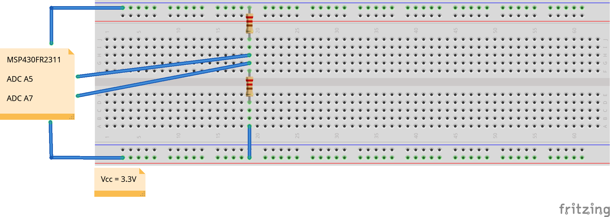
I have a problem with my ADC reading on the msp430fr2311. I have two ADC (A5 and A7) running, and they work perfectly fine if I am reading out 3.3 V or 0V directly. Since my final design requires a voltage devider to trimm the analog output (read value for ADC), I set up a voltage devider on my breadboard which is dividing the voltage by 2 (see below). This divider is doing his job and splits my 3.3 V equally.

If I connect now the ADCs (doesnt matter if one or both) then the voltage drops from 1.65 to 0.14 V.. What am I doing wrong here? I tried it with different resistors and also treated the ADC input as another resistor parallel to the second one.. still no change. I really need your help. If you reqire further infos, please let me know.

Best wishes

Fabi

  • The ADC inputs have limits on source resistance because you have to charge the sampling capacitance during the sampling time. The documentation has all the details.

  • Hey David,

    thank you for your reply. Do you mean the resistance in the table below? Which one is it?

    Thanks for your help.

  • High impedance inputs fill the sampling capacitor more slowly, so you need a longer sample/hold period. 

    The solution is to increase the SHT setting in the ADC and/or reduce the resistor values in your divider. User Guide (SLAU445I) Sec 21.2.5.3 gives a formula for computing the sample/hold time based on the circuit parameters. As a first experiment, just set SHT really high and see if it changes your result.

  • What are the value of the resistors?

  • Hi Bruce,

    thanks for your reply. My problem is not the ADC measurement since I am verifing my voltages with a multimeter.

    I added some information to my current set up. If do not have the ADC connected between R1 and R2 everything is fine. I measure 1.65 V at R2: cool, voltage devider works. Now I plug in the ADC in between the R1 and R2 to measure the 1.65V (U2), but the voltage drops to 0.1V.

    From the section User Guide (SLAU445I) Sec 21.2.5.3 i can see, that there is an input R = Internal MUX-on input resistance which is suppose to be 2k Ohm. But this cant be if i consider the measured voltages.

    So, i even dont use my ADC at this point. I just connect it and see this voltage drop. The funny part is, if let him measrue, the measruement of 0.1V is correct red.

  • Until you configure the port to be used with the ADC it is just a GPIO port which is fully capable of pulling the pin down if set that way.

  • My pins are configured and the MSP430 is running. If i measure other voltages without the voltage divider, i do not have problems.

    They appear only if I set up the above voltage devider.

  • Hey Keith, please see the graphic below your answer.

  • How (exactly) are the pins configured? What (exactly) is your MCU doing when it's running? What platform are you using? (Launchpad?)

    This is an unusual symptom, so I'm suspecting you're doing something unusual.

    If you can post/attach your code maybe someone will see something. Sometimes all it takes is a typo.

  • Hi Bruce,
    this is my ADC.c file, where I have my adc functions defined.

    myADC.c

    #include <msp430.h> #include "driverlib/MSP430FR2xx_4xx/driverlib.h" /************************************************************************************************** * @fn enable_ADC5 * * @brief Enables the ADC on Port 1 A5 -> Pin 1.5 * * @param void * * @return void **************************************************************************************************/ void enable_ADC5(void){ //Initialize the ADC Module /* * Base Address for the ADC Module * Use internal ADC bit as sample/hold signal to start conversion * USE MODOSC 5MHZ Digital Oscillator as clock source * Use default clock divider of 1 */ ADC_init(ADC_BASE, ADC_SAMPLEHOLDSOURCE_SC, ADC_CLOCKSOURCE_ADCOSC, ADC_CLOCKDIVIDER_1); ADC_enable(ADC_BASE); /* * Base Address for the ADC Module * Sample/hold for 16 clock cycles * Do not enable Multiple Sampling */ ADC_setupSamplingTimer(ADC_BASE, ADC_CYCLEHOLD_16_CYCLES, ADC_MULTIPLESAMPLESDISABLE); //Configure the Memory Buffer /* * Base Address for the ADC Module * Use input A5 * Use positive reference of AVcc * Use negative reference of AVss */ ADC_configureMemory(ADC_BASE, ADC_INPUT_A5, ADC_VREFPOS_AVCC, ADC_VREFNEG_AVSS); ADC_clearInterrupt(ADC_BASE, ADC_COMPLETED_INTERRUPT); //Enable the Memory Buffer Interrupt ADC_enableInterrupt(ADC_BASE, ADC_COMPLETED_INTERRUPT); } /************************************************************************************************** * @fn enable_ADC6 * * @brief Enables the ADC on Port 1 A6 -> Pin 1.6 * * @param void * * @return void **************************************************************************************************/ void enable_ADC7(void){ //Initialize the ADC Module /* * Base Address for the ADC Module * Use internal ADC bit as sample/hold signal to start conversion * USE MODOSC 5MHZ Digital Oscillator as clock source * Use default clock divider of 1 */ ADC_init(ADC_BASE, ADC_SAMPLEHOLDSOURCE_SC, ADC_CLOCKSOURCE_ADCOSC, ADC_CLOCKDIVIDER_1); ADC_enable(ADC_BASE); /* * Base Address for the ADC Module * Sample/hold for 16 clock cycles * Do not enable Multiple Sampling */ ADC_setupSamplingTimer(ADC_BASE, ADC_CYCLEHOLD_16_CYCLES, ADC_MULTIPLESAMPLESDISABLE); //Configure the Memory Buffer /* * Base Address for the ADC Module * Use input A7 * Use positive reference of AVcc * Use negative reference of AVss */ ADC_configureMemory(ADC_BASE, ADC_INPUT_A7, ADC_VREFPOS_AVCC, ADC_VREFNEG_AVSS); ADC_clearInterrupt(ADC_BASE, ADC_COMPLETED_INTERRUPT); //Enable the Memory Buffer Interrupt ADC_enableInterrupt(ADC_BASE, ADC_COMPLETED_INTERRUPT); } /************************************************************************************************** * @fn disable_ADC * * @brief Disables the ADC in general * * @param void * * @return void **************************************************************************************************/ void disable_ADC(void){ ADC_disableConversions(ADC_BASE,0); ADC_disable(ADC_BASE); } /************************************************************************************************** * @fn sample_ADC5 * * @brief Reads the ADC on Port 1 A5 -> Pin 1.5 * * @param void * * @return void **************************************************************************************************/ void sample_ADC5(void){ /* Enables the ADC and make the setup */ enable_ADC5(); /* Waits 15 cycles for ADC to set up */ __delay_cycles(15); /* Enable and Start the conversion in Single-Channel, Single Conversion Mode*/ ADC_startConversion(ADC_BASE, ADC_SINGLECHANNEL); /* LPM3, ADC conversion complete will force exit */ __bis_SR_register(LPM3_bits + GIE); /* Cleares the ADC */ disable_ADC(); } /************************************************************************************************** * @fn sample_ADC6 * * @brief Reads the ADC on Port 1 A6 -> Pin 1.6 * * @param void * * @return void **************************************************************************************************/ void sample_ADC6(void){ /* Enables the ADC and make the setup */ enable_ADC6(); /* Waits 15 cycles for ADC to set up */ __delay_cycles(15); /* Enable and Start the conversion in Single-Channel, Single Conversion Mode*/ ADC_startConversion(ADC_BASE, ADC_SINGLECHANNEL); /* LPM3, ADC conversion complete will force exit */ __bis_SR_register(LPM3_bits + GIE); /* Cleares the ADC */ disable_ADC(); }

    And this is my main.c file:
    /* ------------------------------------------------------------------------------------------------
     *                                          Includes
     * ------------------------------------------------------------------------------------------------
     */
    #include <msp430.h>
    #include <stdbool.h>
    #include "driverlib/MSP430FR2xx_4xx/driverlib.h"
    #include "VoltLib/voltLib.h"
    
    /* ------------------------------------------------------------------------------------------------
    *                                           Constants
    * ------------------------------------------------------------------------------------------------
    */
    
    
    /* ------------------------------------------------------------------------------------------------
    *                                           Globals
    * ------------------------------------------------------------------------------------------------
    */
    /* Timer 120 sec */
    uint8_t Timer_120_cnt = 0;
    bool Timer_120_flag = false;
    
    /* ADC variables 
    *  ADC conversion result 0 - 1023 ( 0h - 0ffh)
    */
    int ADC_Conversion_Result = 0;
    float ADC_factor = 0.0032;
    float _arr_ADC_voltage[5];
    float ADC_voltage_cal = 0;
    float ADC_voltage_sum = 0;
    float ADC_voltage = 0;
    
    /* I2C 
    *  TXData = the databyte to send
    *  TXByteCtr = additional byte number for sending multiple bytes as I2C master. See ISR
    */
    int DAC0_TXdata = 0;
    uint8_t TXData0 = 0x00;
    uint8_t TXData1 = 0x00;
    uint8_t TXByteCtr = 1;
    
    
    int main(void)
    {
        
        
        /*
        1. Initialization
        */
        // Stop the watchdog timer
        WDTCTL = WDTPW | WDTHOLD;
        initGPIO();
        initTimerB(32768);
        initI2C();
        
        while(1){
            /* Enter low power mode 3 with gi enabled */
            __bis_SR_register(LPM3_bits + GIE);
            
            /* Request the timer. If flag is set, start the measurement and send the data via I2C */
            if(Timer_120_flag){
                
                /*------------------------------------------------------------------
                *                           Read ADC5 
                ------------------------------------------------------------------*/
                
                /* If timer pings, take 5 samples and write them into the array */
                int i = 0;
                for(i=0; i<5; i++){
                    /* Read the ADC */
                    sample_ADC5();
                    /* Calculate the actual value */
                    ADC_voltage_cal = (ADC_factor * ADC_Conversion_Result);
                    /* Write the value in the array */
                    _arr_ADC_voltage[i] = ADC_voltage_cal;
                }
                
                /* Get the avarage of the array. Fixed size to 5 */
                ADC_voltage = ADC_avarage(_arr_ADC_voltage);
                
                
                /*------------------------------------------------------------------
                *                           Read ADC7 
                ------------------------------------------------------------------*/
                
                // Try ADC 6 ( second one)
                /* If timer pings, take 5 samples and write them into the array */
                for(i=0; i<5; i++){
                    /* Read the ADC */
                    sample_ADC6();
                    /* Calculate the actual value */
                    ADC_voltage_cal = (ADC_factor * ADC_Conversion_Result);
                    /* Write the value in the array */
                    _arr_ADC_voltage[i] = ADC_voltage_cal;
                }
                
                /* Get the avarage of the array. Fixed size to 5 */
                ADC_voltage = ADC_avarage(_arr_ADC_voltage);
                
            }
            
            
        }
        
    	return 0;
    }
    
    /* ------------------------------------------------------------------------------------------------
    *                                           ISRs
    * ------------------------------------------------------------------------------------------------
    */
    /* ADC interrupt service routine 
    * ------------------------------------------------------------------------------------------------
    */
    #if defined(__TI_COMPILER_VERSION__) || defined(__IAR_SYSTEMS_ICC__)
    #pragma vector=ADC_VECTOR
    __interrupt void ADC_ISR(void)
    #elif defined(__GNUC__)
    void __attribute__ ((interrupt(ADC_VECTOR))) ADC_ISR (void)
    #else
    #error Compiler not supported!
    #endif
    {
        //Get previous write protection setting
        uint8_t state = HWREG8(SYS_BASE + OFS_SYSCFG0_L);
    #ifdef DFWP
        uint8_t wp = DFWP | PFWP;
    #else
        uint8_t wp = PFWP;
    #endif
    
    #ifdef FRWPPW
        HWREG16(SYS_BASE + OFS_SYSCFG0) = FWPW | (state & ~wp);
    #else
        HWREG8(SYS_BASE + OFS_SYSCFG0_L) &= ~wp;
    #endif
        
        // Get conversion result
        ADC_Conversion_Result = ADCMEM0;
    
    
        //Restore previous write protection setting
    #ifdef FRWPPW
        HWREG16(SYS_BASE + OFS_SYSCFG0) = FWPW | state;
    #else
        HWREG8(SYS_BASE + OFS_SYSCFG0_L) = state;
    #endif
        // Sleep Timer Exits LPM3
    	__bic_SR_register_on_exit(LPM3_bits);              
    }
    
    
    I have a timer running and after some seconds i run the sampling. As i said, without the voltage devider i can measure the correct voltages. I think it is an anlog problem regarding the input inpedance of the ADC. But i honestly dont understand it. 


  • The ADC_init() function doesn't alter the pin configuration so it will remain whatever your initGPIO() function set it to.

  • It looks as though initGPIO() has something interesting in it. I'm looking for a line resembling:

    > GPIO_setAsPeripheralModuleFunctionInputPin(GPIO_PORT_P1, GPIO_PIN5|GPIO_PIN7, GPIO_TERNARY_MODULE_FUNCTION); // A5/7

    Also, if you're using the Launchpad, don't forget to remove the RXD/TXD jumpers from J101 ("bridge" header). I'm not exactly sure what the other end of TXD looks like.

  • Hi guys,

    in the end i think i will just place an opamp before my ADC instead of the voltage devider.

    Maybe because of the input impedance of the ADC I have to recalculate the offset / gain of my ADC. I thought it would be easier and I can just measure the voltage directly.

    Best

    Fabi

  • I just set up a similar experiment on a Launchpad, and I didn't see your symptom.

    I constructed a "flying register" divider (1K+1K) across 3V3 and GND, and fed the midpoint into P1.5 and P1.7 (one at a time). 

    I constructed an initGPIO() function which optionally includes that line of code above.  I didn't add the timer code required to actually run the ADC, so the program just sits in LPM3.

    With or without that line, my DMM sees 1.65V at the tap location (connected to either P1.5 or P1.7).

    I suspect there's something else (not shown) going on. I still wonder what your initGPIO() function does.

    [Edit: Fixed typo]

  • Hi Bruce,

    many thanks for your support. You can see my initGPIO() function here. This is my first project with the msp430 so excuse studpid mistakes.. maybe you could also post your code, so i can compare the settings made. Maybe it is also sth with my GPIO settings..

    #include <msp430.h>
    #include "driverlib/MSP430FR2xx_4xx/driverlib.h"
    
    void initGPIO(void){
        /*
        PxDIR -> Port x direction
        PxOUT -> Port x output
        */
        P1DIR |= 0xFF;
        P1OUT = 0x00;
        P2DIR |= 0xFF;
        P2OUT = 0x00;
        
        GPIO_setAsOutputPin(GPIO_PORT_P1,GPIO_PIN0);
        GPIO_setOutputLowOnPin(GPIO_PORT_P1,GPIO_PIN0);
        
        //Set A5 as an input pin.
        //Set appropriate module function
        /*GPIO_setAsPeripheralModuleFunctionInputPin(
                GPIO_PORT_P1,
                GPIO_PIN5,
                GPIO_TERNARY_MODULE_FUNCTION);*/
        
    
        /* I2C init */
        GPIO_setAsPeripheralModuleFunctionInputPin(
            GPIO_PORT_P1,
            GPIO_PIN2 + GPIO_PIN3,
            GPIO_PRIMARY_MODULE_FUNCTION
        );
    
        
        /*
         * Disable the GPIO power-on default high-impedance mode to activate
         * previously configured port settings
         */
        PMM_unlockLPM5();


        /*
        Mark the correct initialization
        */
        GPIO_toggleOutputOnPin(GPIO_PORT_P1, GPIO_PIN0);
        __delay_cycles(30000);
        GPIO_toggleOutputOnPin(GPIO_PORT_P1, GPIO_PIN0);
    }
    

  • >    P1DIR |= 0xFF;
    >    P1OUT = 0x00;
    This drives P1.5/7 low, so you'll read low at A5/A7 (give or take a minor fight with the divider).
    The line of code I mentioned is commented out, so it isn't really there. When I un-comment it, I get correct behavior on A5 (but not A7).
    I recommend that you insert the line of code I mentioned (which configures both pins) and leave it there. That call will un-do the P1DIR setting above it, though to be correct you should have something more like this so you don't have even a few microseconds of bus contention:
    >       P1DIR |= 0xFF & ~(BIT5 | BIT7);    // All output except A5/A7
    [Edit: More dispute with the Forum formatter]
  • Bruce the almighty!! Thats working man! Thanks a lot!

    I thought the settings for the GPIO would be overwritten with the standard settings for the ADC pin.

    I also tried this, but it didnt help.

    //Set A7 as an input pin.
        //Set appropriate module function
        GPIO_setAsPeripheralModuleFunctionInputPin(
                GPIO_PORT_ADC7,
                GPIO_PIN_ADC7,
                GPIO_FUNCTION_ADC7);

    I love the support, thanks guys, especially bruce! Have blessed days!

**Attention** This is a public forum