


Hi,
I'm new at this and a would like to know when I do the initialization of spi:
What is the secondary function ?
What is doing this line of code?
P4SEL |= BIT3+BIT4; // P4.3,4 option select
P4SEL |= BIT0; // P4.0 option select
How to set a bit in '0'?
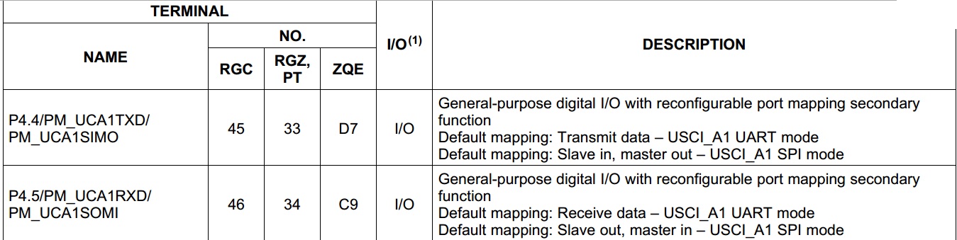
From datasheet those pins have 3 functions? how to chose USCI_A1 UART mode?
Regards David.

