This thread has been locked.

If you have a related question, please click the "Ask a related question" button in the top right corner. The newly created question will be automatically linked to this question.

MSP430FR2355: Code for indicators

Part Number: MSP430FR2355
Other Parts Discussed in Thread: TIDA-010056, , DRV8350R, DRV8323

Hello TI helpers,

We're using TIDA-010056 as reference code. We connected switches at P3.3 and P3.4 for left and right indicator respectively. We tried to write our own code in main loop but we show that whenever we pressed switch, execution of main code stopped and only respective indicator worked. It means motor(here we connect bulbs instead of motor for testing purpose) stops for a while and only indicators work but that we don't want it.. 

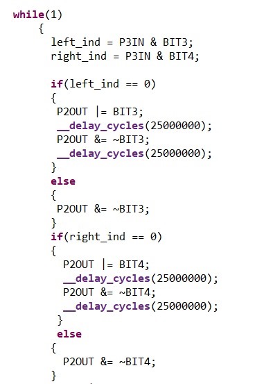
Here is the our code for indicators.

  we want both code runs simultaneously... please help us it will be great help.

Thank you in advance.

  • Are you just looking for something like:

    unsigned char bits_to_set = 0;
    if (left_ind == 0)  bits_to_set |= BIT3;
    if (right_ind == 0) bits_to_set |= BIT4;
    if (bits_to_set != 0)
    {
        P2OUT |= bits_to_set;      // On
        __delay_cycles(25000000);  // Pause
        P2OUT &= ~bits_to_set;     // Off
        __delay_cycles(25000000);  // Pause
    }
    P2OUT &= ~(BIT3|BIT4);         // All off

  • Thank you for your quick response,

    This code and our code both are executed successfully but our main concern is while executing this code our main code which runs motor is stopped for a while...I think this happens due to __delay_cycles function...

  • /* --COPYRIGHT--,

     * Copyright (c) 2019, Texas Instruments Incorporated

     * All rights reserved.

     *Modified by : A0132403

     *Modified Date: 30th April 2019

     *Modified * Redistribution and use in source and binary forms, with or without

     * modification, are permitted provided that the following conditions

     * are met:

     *

     * * Redistributions of source code must retain the above copyright

     * notice, this list of conditions and the following disclaimer.

     *

     * * Redistributions in binary form must reproduce the above copyright

     * notice, this list of conditions and the following disclaimer in the

     * documentation and/or other materials provided with the distribution.

     *

     * * Neither the name of Texas Instruments Incorporated nor the names of

     * its contributors may be used to endorse or promote products derived

     * from this software without specific prior written permission.

     * THIS SOFTWARE IS PROVIDED BY THE COPYRIGHT HOLDERS AND CONTRIBUTORS "AS IS"

     * AND ANY EXPRESS OR IMPLIED WARRANTIES, INCLUDING, BUT NOT LIMITED TO,

     * THE IMPLIED WARRANTIES OF MERCHANTABILITY AND FITNESS FOR A PARTICULAR

     * PURPOSE ARE DISCLAIMED. IN NO EVENT SHALL THE COPYRIGHT OWNER OR

     * CONTRIBUTORS BE LIABLE FOR ANY DIRECT, INDIRECT, INCIDENTAL, SPECIAL,

     * EXEMPLARY, OR CONSEQUENTIAL DAMAGES (INCLUDING, BUT NOT LIMITED TO,

     * PROCUREMENT OF SUBSTITUTE GOODS OR SERVICES; LOSS OF USE, DATA, OR PROFITS;

     * OR BUSINESS INTERRUPTION) HOWEVER CAUSED AND ON ANY THEORY OF LIABILITY,

     * WHETHER IN CONTRACT, STRICT LIABILITY, OR TORT (INCLUDING NEGLIGENCE OR

     * OTHERWISE) ARISING IN ANY WAY OUT OF THE USE OF THIS SOFTWARE,

     * EVEN IF ADVISED OF THE POSSIBILITY OF SUCH DAMAGE.

     *

    *****************************

    // System Configuration

    // Device Part Number : MSP430FR2355

    // compiler : Code Composer Studio v8.3.0

    // Oscillator Frequency : 24MHz, using internal DCO

    // PWM generation : TIMER: TB3.1 –TB.6, Clock = 25 MHz, PWM frequency set for 20kHz

    20 kHz

    //

    // Position Feedback : Hall sensors signals

    // HA -> P3.0

    // HB -> P3.1

    // HC -> P3.2

     *

    // ADC : A0 -> Speed reference from the external potentiometer/trigger

    // A6 -> Phase A back EMF sensing for sensorless

    // A5 -> Phase B back EMF sensing for sensorless

    // A4 -> Phase C back EMF sensing for sensorless

    // A7 -> DC bus voltage sensing

    // A8 -> Low-side DC bus current sensing

    // A9 -> PCB or FET temperature feedback

     *

     *

    //Comparator configuration for back EMF zero crossing detection : CB2/P1.2 -> IDC

    // COMP0.O (P2.0) – Phase A back EMF zero cross comparator

    // COMP1.O(P2.1) – Phase C back EMF zero cross comparator

    // OA1O (P1.5) - Phase C back EMF zero cross comparator. The

    //opamp of smart compo module is configured as a comparator

    *

    //DRV8350RS - SPI programming pins connection /B1

    // P4.4 -> SCS

    // P4.5 -> SCLK

    // P4.6 -> SDO

    // P4.7 -> SDI

     *

    //UART communication

    // P4.2 -> UART RX pin

    // P4.3 -> UART TX pin

    //MCU Digital Inputs/Output

    // P5.4 -> Direction of motor rotation

    // P4.1 -> ENABLE connection for DRV8350R

    // P4.0 -> FAULT pin connection from DRV8350R

    // P2.6 -> LED output

    *****************************/

    //Header Files//

    #include "msp430fr2355.h"

    #include "stdint.h"

    #define CALTDH0CTL1_256 *((unsigned int *)0x1A36)

    /**********InstaSPIN*************/

    #define PWM_PERIOD 600 //PWM Frequency (Hz) = 25MHz/((2*PWM_PERIOD)-1)

    #define MAX_DUTYCYCLE 600 //relative to PWM_PERIOD

    #define MIN_DUTYCYCLE 5 //relative to PWM_PERIOD

    #define ACCEL_RATE 100 //Ramp up time to full scale duty cycle = (Full scale duty cycle) * ACCEL_RATE * PWM_PERIOD/PWM_Frequency

    #define DEAD_TIME_MCU 1 // Dead time from MSP430 = DEAD_TIME* 0.0625 uS (for 16MHz clock)

    #define Block_Rotor_Duration 800 //Blocked_rotor shut off time (s) = Block_Rotor_Duration*30000/Timer clock frequency

    /************program variables***************/

    unsigned int DC_BUS_CURRENT = 0;

    unsigned int DC_Bus_Voltage = 0;

    unsigned int SPEED_REF = 0;

    unsigned int Temperature_feedback = 0;

    unsigned int start_count = 0;

    unsigned int HALL_STATE = 0;

    unsigned int softstart_counter = 0;

    unsigned int CurrentDutyCycle = 100;

    unsigned int DIRECTION = 0 ;

    unsigned int FirstADC_flag = 1;

    unsigned int ADC_selection_flag = 1;

    unsigned int ADC_selection_flag_1 = 1;

    unsigned int Block_Rotor_Counter = 0;

    unsigned int Block_Rotor_Counter_1 =0;

    unsigned int ADC_RESULT = 0;

    unsigned int commutation_time = 0;

    unsigned int commutation_time_counter = 0;

    unsigned int advance_angle_time_counter = 0;

    unsigned int advance_angle_time = 0;

    unsigned int commutation_done = 0;

    unsigned int Previous_State = 0;

    unsigned int Present_State = 0;

    unsigned int PWM_DUTY = PWM_PERIOD;

    unsigned int left_ind;

    unsigned int right_ind;

    /**********ADC channel selection**************/

    #define MEASURE_SPEED \

                                    ADCCTL0 |= ADCSHT_2 | ADCON; \

                                    ADCCTL1 |= ADCSHP; \

                                    ADCCTL2 &= ~ADCRES; \

                                    ADCCTL2 |= ADCRES_2; \

                                    ADCMCTL0 |= ADCINCH_0; \

                                    ADCIE = ADCIE0;

    #define MEASURE_TEMP \

                                    ADCCTL0 |= ADCSHT_2 | ADCON; \

                                    ADCCTL1 |= ADCSHP; \

                                    ADCCTL2 &= ~ADCRES; \

                                    ADCCTL2 |= ADCRES_2; \

                                    ADCMCTL0 |= ADCINCH_9; \

                                    ADCIE = ADCIE0;

    #define MEASURE_VDC \

                                    ADCCTL0 |= ADCSHT_2 | ADCON; \

                                    ADCCTL1 |= ADCSHP; \

                                    ADCCTL2 &= ~ADCRES; \

                                    ADCCTL2 |= ADCRES_2; \

                                    ADCMCTL0 |= ADCINCH_7; \

                                    ADCIE = ADCIE0;

    #define MEASURE_IDC \

                                    ADCCTL0 |= ADCSHT_2 | ADCON; \

                                    ADCCTL1 |= ADCSHP; \

                                    ADCCTL2 &= ~ADCRES; \

                                    ADCCTL2 |= ADCRES_2; \

                                    ADCMCTL0 |= ADCINCH_8; \

                                    ADCIE = ADCIE0;

    #define MEASURE_BEMF_A \

                                    ADCCTL0 |= ADCSHT_2 | ADCON; \

                                    ADCCTL1 |= ADCSHP; \

                                    ADCCTL2 &= ~ADCRES; \

                                    ADCCTL2 |= ADCRES_2; \

                                    ADCMCTL0 |= ADCINCH_6; \

                                    ADCIE = ADCIE0;

    #define MEASURE_BEMF_B \

                                    ADCCTL0 |= ADCSHT_2 | ADCON; \

                                    ADCCTL1 |= ADCSHP; \

                                    ADCCTL2 &= ~ADCRES; \

                                    ADCCTL2 |= ADCRES_2; \

                                    ADCMCTL0 |= ADCINCH_5; \

                                    ADCIE = ADCIE0;

    #define MEASURE_BEMF_C \

                                    ADCCTL0 |= ADCSHT_2 | ADCON; \

                                    ADCCTL1 |= ADCSHP; \

                                    ADCCTL2 &= ~ADCRES; \

                                    ADCCTL2 |= ADCRES_2; \

                                    ADCMCTL0 |= ADCINCH_4; \

                                    ADCIE = ADCIE0;

    #define CONVERSION_ENABLE \

                                    ADCCTL0 |= ADCENC | ADCSC;

    #define CONVERSION_DISABLE \

                                    ADCCTL0 &= ~ADCENC; \

                                    ADCCTL1 = 0;

    /**********END OF ADC channel selection**************/

    int LPM3_On = 0;

    void Init_Clocks (void);

    void init_IO (void);

    void init_WDT (void);

    void init_ADC (void);

    void init_TimerB (void);

    void Hall_State_Change_FORWARD(void);

    void Hall_State_Change_REVERSE(void);

    void A_PWM(void);

    void B_PWM(void);

    void C_PWM(void);

    void A_LOW(void);

    void B_LOW(void);

    void C_LOW(void);

    void A_Z(void);

    void B_Z(void);

    void C_Z(void);

    void A_HIGH(void);

    void B_HIGH(void);

    void C_HIGH(void);

    void main (void)

    {

        WDTCTL = WDTPW + WDTHOLD; // Stop WDT

        _delay_cycles(1000000);

        Init_Clocks (); // Initialize clocks for 25 MHz

        init_ADC ();

        init_TimerB ();

        init_WDT();

        init_IO ();

        A_Z();

        B_Z();

        C_Z();

        __delay_cycles(1000000);

        /***********ENABLE for DRV8323******************/

                P4OUT &= ~BIT1;

                __delay_cycles(2500); //100 us delay

                P4OUT |= BIT1; // DELAY CYCLES MA CHANGES KARYA CH 07/04/2021 NA ROJ

                __delay_cycles(250); //10 us delay

        DIRECTION = (P5IN & BIT4);

        HALL_STATE = ((P3IN & BIT0) + (P3IN & BIT1) + (P3IN & BIT2));

        P3DIR &= ~BIT3; // left_indicator as input

        P3REN |= BIT3;

        P3OUT |= BIT3;

        P3IES |= BIT3;

        P3DIR &= ~BIT4; // right_indicator as input

        P3REN |= BIT4;

        P3OUT |= BIT4;

        P3IES |= BIT4;

        P2DIR |= BIT3; // relay 1 as output

        P2DIR |= BIT4; // relay 2 as output

     /* //-- setup timer timer0_b3

        TB0CTL |= TBCLR;

        TB0CTL |= MC__UP;

        TB0CTL |= TBSSEL__ACLK;

        TB0CCR0 = 32768;*/

        unsigned char bits_to_set = 0;

        // ---- Brake System

        P5DIR &= ~BIT3; // left_brake as input

        P5REN |= BIT3;

        P5OUT |= BIT3;

        P5IES |= BIT3;

        P5DIR &= ~BIT2; // right_brake as input

        P5REN |= BIT2;

        P5OUT |= BIT2;

        P5IES |= BIT2;

    /* //-- SETUP TIMER COMPARE IRQ

        TB0CCTL0 |= CCIE;

        __enable_interrupt();

        TB0CCTL0 &= ~CCIFG;

        //-- setup IRQs

        P3IE |= BIT3;

        P3IE |= BIT4;

        __enable_interrupt();

        P3IFG &= ~ BIT3;

        P3IFG &= ~ BIT4;*/

        __enable_interrupt();

        P5IE |= BIT3;

        P5IE |= BIT2;

        P5IFG &= ~ BIT3;

        P5IFG &= ~ BIT2;

        P4DIR |= BIT0;

        P4DIR |= BIT1;

        P6DIR |= BIT0;

        P6DIR |= BIT1;

        P6DIR |= BIT2;

        P6DIR |= BIT3;

        P6DIR |= BIT4;

        P6DIR |= BIT5;

            while(1)

            {

                  P4OUT |= BIT1;

                  P4OUT |= BIT0;

                  P6OUT |= BIT0;

                  P6OUT |= BIT1;

                  P6OUT |= BIT2;

                  P6OUT &= ~BIT3;

                  P6OUT |= BIT4;

                  P6OUT |= BIT5;


                  if (left_ind == 0) bits_to_set |= BIT3;

                  if (right_ind == 0) bits_to_set |= BIT4;

                  if (bits_to_set != 0)

                  {

                      P3OUT |= bits_to_set; // On

                      __delay_cycles(25000000); // Pause

                      P3OUT &= ~bits_to_set; // Off

                      __delay_cycles(25000000); // Pause

                  }

                  P3OUT &= ~(BIT3|BIT4); // All off

                  }

              // if(softstart_counter >= ACCEL_RATE)

                // {

                        softstart_counter = 0;

                        if (CurrentDutyCycle < SPEED_REF)

                        {

                            CurrentDutyCycle ++;

                        }

                        else if (CurrentDutyCycle > SPEED_REF)

                        {

                            CurrentDutyCycle --;

                        }

                        if ( CurrentDutyCycle >= MAX_DUTYCYCLE)

                        {

                            CurrentDutyCycle = MAX_DUTYCYCLE;

                        }

                        else if (CurrentDutyCycle <= MIN_DUTYCYCLE)

                        {

                            CurrentDutyCycle = MIN_DUTYCYCLE;

                        }

                // }

                if(DIRECTION == 0)

                {

                    Hall_State_Change_FORWARD();

                }

                else

                {

                    Hall_State_Change_REVERSE();

                }

                }

    }

    //end main

    //-- ISRs----//

    #pragma vector = TIMER0_B0_VECTOR

    __interrupt void ISR_TB0_CCR0(void)

    {

        P2OUT ^= BIT3;

        P2OUT ^= BIT4;

        TB0CCTL0 &= ~CCIFG;

    }

    #pragma vector=PORT5_VECTOR

    __interrupt void Port_5(void)

    {

    }

    //WDT to restart ADC

     void init_WDT (void)

    {

          WDTCTL = WDT_MDLY_32; // WDT 32ms from 1MHz, SMCLK, interval time

          SFRIE1 |= WDTIE; // Enable WDT interrupt

    }

    void init_TimerB (void)

        {

            TB3CTL = TBSSEL__SMCLK | MC_3 | TBCLR; // SMCLK, up_down mode, clear TBR

            TB3CCR0 = PWM_PERIOD; // PWM Period

            TB3CCR1 = PWM_PERIOD; // CCR1 PWM duty cycle

            /*TB3CCR2 = PWM_PERIOD; // CCR2 PWM duty cycle

            TB3CCR3 = PWM_PERIOD; // CCR3 PWM duty cycle

            TB3CCR4 = PWM_PERIOD; // CCR4 PWM duty cycle

            TB3CCR5 = PWM_PERIOD; // CCR3 PWM duty cycle

            TB3CCR6 = PWM_PERIOD; // CCR4 PWM duty cycle*/

            TB3CCTL1 = OUTMOD_6; // CCR1 reset/set

            /*TB3CCTL2 = OUTMOD_2; // CCR2 reset/set

            TB3CCTL3 = OUTMOD_6; // CCR3 reset/set

            TB3CCTL4 = OUTMOD_2; // CCR4 reset/set

            TB3CCTL5 = OUTMOD_6; // CCR4 reset/set

            TB3CCTL6 = OUTMOD_2; // CCR4 reset/set*/

            TB3CCTL0 |= CCIE;

           // TB3CCTL1 |= CCIE;

          __bis_SR_register(GIE); // enable interrupts

          __no_operation(); // For debugger

            _EINT(); // Enable interrupts

        }

    // Clocks And Vcore

    void Init_Clocks (void)

    {

        FRCTL0 = FRCTLPW | NWAITS_2;

        __bis_SR_register(SCG0); // disable FLL

        CSCTL3 |= SELREF__REFOCLK; // Set REFO as FLL reference source

        CSCTL0 = 0; // clear DCO and MOD registers

        CSCTL1 |= DCORSEL_7; // Set DCO = 24MHz

        CSCTL2 = FLLD_0 + 731; // DCOCLKDIV = 24MHz

        __delay_cycles(3);

        __bic_SR_register(SCG0); // enable FLL

        while(CSCTL7 & (FLLUNLOCK0 | FLLUNLOCK1)); // FLL locked

        CSCTL4 = SELMS__DCOCLKDIV | SELA__REFOCLK; // set default REFO(~32768Hz) as ACLK source, ACLK = 32768Hz

                                                           // default DCOCLKDIV as MCLK and SMCLK source

    }

    //IO INITIALISATION//

    void init_IO (void)

        {

            //Hall Sensor inputs

            P3SEL0 &= ~(BIT0+BIT1+BIT2); //GPIO - Hall sensors

            P3DIR &= ~(BIT0+BIT1+BIT2); //Inputs - Hall sensors

            //PWM outputs

            //GPIO-PWM

            P6DIR |= (BIT0+BIT1+BIT2+BIT3+BIT4+BIT5); //OutputPWM

            //Indications

            P2SEL0 &= ~ (BIT6); //GPIO-LED3

            P2DIR |= (BIT6); //Output-LED3

            //Direction Control

            P5SEL0 &= ~(BIT4); //GPIO - DIR

            P5DIR &= ~(BIT4); //Input - DIR

            //Enable Gate driver

            P4SEL0 &= ~(BIT1); //GPIO - DIR

            P4DIR |= (BIT1); //Input - DIR

            //Fault input

            P4SEL0 &= ~(BIT0); //GPIO - DIR

            P4DIR &= ~(BIT0); //Input - DIR

            //Enable edge interrupt for Hall sensor ports

            P3IES |= ((BIT0)+(BIT1)+(BIT2)); // change the hall interrupt to falling edge to detect both the edges

            P3IE |= (BIT0 | BIT1 | BIT2);

            PM5CTL0 &= ~LOCKLPM5;

            P3IFG &= ~(BIT0| BIT1 | BIT2);

            __bis_SR_register(GIE);

        }

    void init_ADC (void)

    {

        // Configure ADC12

        ADCCTL0 |= ADCSHT_2 | ADCON; // ADCON, S&H=16 ADC clks

        ADCCTL1 |= ADCSHP; // ADCCLK = MODOSC; sampling timer

        ADCCTL2 &= ~ADCRES; // clear ADCRES in ADCCTL

        ADCCTL2 |= ADCRES_2; // 12-bit conversion results

        ADCMCTL0 |= ADCINCH_0; // A1 ADC input select; Vref=AVCC

        ADCIE |= ADCIE0; // Enable ADC conv complete interrupt

    }

    /*************TIMERD0.1 INTERRUPT***************/

    // Timer B1 interrupt service routine

    #pragma vector = TIMER3_B1_VECTOR

    __interrupt void Timer3_B1_ISR(void)

    {

          PWM_DUTY = (PWM_PERIOD - CurrentDutyCycle);

          /*TB3CCR1 = PWM_DUTY; // CCR1 PWM duty cycle

          TB3CCR2 = PWM_DUTY;

          TB3CCR3 = PWM_DUTY; // CCR1 PWM duty cycle

          TB3CCR4 = PWM_DUTY;

          TB3CCR5 = PWM_DUTY; // CCR1 PWM duty cycle

          TB3CCR6 = PWM_DUTY;*/

              MEASURE_SPEED

              CONVERSION_ENABLE

              TB3CCR1 = PWM_DUTY; // CCR1 PWM duty cycle

              P6OUT &= ~ BIT0;

              TB3CCTL1 &= ~CCIFG;

          /* softstart_counter ++;

              Block_Rotor_Counter_1++;

              if(Block_Rotor_Counter_1>=30000)

              {

                  Block_Rotor_Counter++;

              }

              if (Block_Rotor_Counter > Block_Rotor_Duration)

              {

                  A_Z();

                  B_Z();

                  C_Z();

                  _disable_interrupt ();

                  while (1);

              }*/

    }

    #pragma vector = TIMER3_B0_VECTOR

    __interrupt void ISR_TB3_CCR0(void)

    {

        P6OUT |= BIT0;

        TB3CCTL0 &= ~ CCIFG;

    }

    /*************END OF TIMERD0.1 INTERRUPT***************/

    /*************ADC INTERRUPT***************/

    // ADC interrupt service routine

    #pragma vector=ADC_VECTOR

    __interrupt void ADC_ISR(void)

    {

        switch(__even_in_range(ADCIV,ADCIV_ADCIFG))

        {

            case ADCIV_NONE:

                break;

            case ADCIV_ADCOVIFG:

                break;

            case ADCIV_ADCTOVIFG:

                break;

            case ADCIV_ADCHIIFG:

                break;

            case ADCIV_ADCLOIFG:

                break;

            case ADCIV_ADCINIFG:

                break;

            case ADCIV_ADCIFG:

                ADC_RESULT = ADCMEM0;

                SPEED_REF = (ADC_RESULT>>2);

                break;

            default:

                break;

        }

    }

    /***********Port 1 interrupt service routine***********/

    #pragma vector=PORT3_VECTOR

    __interrupt void Port_3(void)

    {

        HALL_STATE = ((P3IN & BIT0) + (P3IN & BIT1) + (P3IN & BIT2));

        if(DIRECTION == 0)

        {

            Hall_State_Change_FORWARD();

        }

        else

        {

            Hall_State_Change_REVERSE();

        }

        Block_Rotor_Counter = 0;

        Block_Rotor_Counter_1 =0;

        P3IES ^= (BIT0)+(BIT1)+(BIT2);

        P3IFG &= ~(BIT0| BIT1 | BIT2);

      /* right_ind = P3IN & BIT4;

          if(right_ind == 0)

          {

              P2OUT ^= BIT4;

          }

          else

          {

              P2OUT &= ~BIT4;

          }

          P3IFG &= ~ BIT4;

          left_ind = P3IN & BIT3;

          if(left_ind == 0)

          {

              P2OUT ^= BIT3;

          }

          else

          {

              P2OUT &= ~BIT3;

          }

          P3IFG &= ~ BIT3;*/

    }

    /***********END OF ADC INTERRUPT**************/

    // Watchdog Timer interrupt service routine

    #pragma vector=WDT_VECTOR

    __interrupt void WDT_ISR(void)

    {

    }

    /*********Commutation sequence Forward****************/

    void Hall_State_Change_FORWARD(void)

    {

                switch (HALL_STATE)

                {

                    case 2:

                            C_Z();

                            A_PWM();

                            B_LOW();

                    break;

                    case 6:

                            B_Z();

                            A_PWM();

                            C_LOW();

                        break;

                    case 3:

                            A_Z();

                            C_PWM();

                            B_LOW();

                            break;

                    case 1:

                            B_Z();

                            C_PWM();

                            A_LOW();

                            break;

                    case 4:

                            A_Z();

                            B_PWM();

                            C_LOW();

                            break;

                    case 5:

                            C_Z();

                            B_PWM();

                            A_LOW();

                            break;

                    default:

                        A_Z();

                        B_Z();

                        C_Z();

                        break;

                }

    }

    /*********Commutation sequence Reverse****************/

    void Hall_State_Change_REVERSE(void)

    {

                switch (HALL_STATE)

                {

                    case 2:

                            C_Z();

                            B_PWM();

                            A_LOW();

                    break;

                    case 6:

                            B_Z();

                            C_PWM();

                            A_LOW();

                        break;

                    case 3:

                            A_Z();

                            B_PWM();

                            C_LOW();

                            break;

                    case 1:

                            B_Z();

                            A_PWM();

                            C_LOW();

                            break;

                    case 4:

                            A_Z();

                            C_PWM();

                            B_LOW();

                            break;

                    case 5:

                            C_Z();

                            A_PWM();

                            B_LOW();

                            break;

                    default:

                        A_Z();

                        B_Z();

                        C_Z();

                        break;

                }

    }

    /*********Definition of PWM GPIOs****************/

    void A_PWM(void)

    {

        P6SEL0 |= BIT0;

        P6SEL0 |= BIT1;

    }

    void B_PWM(void)

    {

        P6SEL0 |= BIT2;

        P6SEL0 |= BIT3;

    }

    void C_PWM(void)

    {

        P6SEL0 |= BIT4;

        P6SEL0 |= BIT5;

    }

    void A_LOW(void)

    {

        P6SEL0 &= ~BIT0;

        P6OUT &= ~BIT0;

        P6SEL0 &= ~BIT1;

        P6OUT |= BIT1;

    }

    void B_LOW(void)

    {

        P6SEL0 &= ~BIT2;

        P6OUT &= ~BIT2;

        P6SEL0 &= ~BIT3;

        P6OUT |= BIT3;

    }

    void C_LOW(void)

    {

        P6SEL0 &= ~BIT4;

        P6OUT &= ~BIT4;

        P6SEL0 &= ~BIT5;

        P6OUT |= BIT5;

    }

    void A_Z(void)

    {

        P6SEL0 &= ~BIT0;

        P6OUT &= ~BIT0;

        P6SEL0 &= ~BIT1;

        P6OUT &= ~BIT1;

    }

    void B_Z(void)

    {

        P6SEL0 &= ~BIT2;

        P6OUT &= ~BIT2;

        P6SEL0 &= ~BIT3;

        P6OUT &= ~BIT3;

    }

    void C_Z(void)

    {

        P6SEL0 &= ~BIT4;

        P6OUT &= ~BIT4;

        P6SEL0 &= ~BIT5;

        P6OUT &= ~BIT5;

    }

    void A_HIGH(void)

    {

        P6SEL0 &= ~BIT0;

        P6OUT |= BIT0;

        P6SEL0 &= ~BIT1;

        P6OUT &= ~BIT1;

    }

    void B_HIGH(void)

    {

        P6SEL0 &= ~BIT2;

        P6OUT |= BIT2;

        P6SEL0 &= ~BIT3;

        P6OUT &= ~BIT3;

    }

    void C_HIGH(void)

    {

        P6SEL0 &= ~BIT4;

        P6OUT |= BIT4;

        P6SEL0 &= ~BIT5;

        P6OUT &= ~BIT5;

    }

    /*********End*********************/

    This is our code....in main(void) function,there is while(1) loop in which our motor run code and indicator code are used ...

  • In order to get rid of the __delay_cycles() you need a scheduler to count the seconds. This doesn't (necessarily) mean an RTOS, you just need some event that can reliably be interpreted as real time. For simple cases, a periodic timer with an interrupt may suffice.

    It looks as though you're running the WDT at a 32ms period (WDT_MDLY_32), so 33x periods is roughly 1 second. A common idiom might look something like:

    __interrupt void WDT_ISR(void)      // Every 32ms
    {
        static int second_counter;
        if (++second_counter >= 1000/32) { // 1000ms/32ms= 1 second
            second_counter = 0;         // Start a new second
            if (bits_to_set == 0)       // No indicators at all
                P3OUT &= ~(BIT3|BIT4);  // All off
            else                        // Input checker in main wants some blinks
                P3OUT ^= bits_to_set;   // Toggle the relevant indicator(s)
        }
    }

    Unsolicited: If you want to post 700+ lines of code, please attach it rather than pasting it. (Insert->Image/video/file).

  • Hello Bruce, 
    Can you briefly explain where we have to write this code ? And how to execute.
    If you give full code it will be great help.
    Thank you in advance.

  • I put it inside the WDT_ISR function in your program, for the reasons I mentioned. It is an example, which you should adapt to your needs. I'm not in a position to write bespoke code for individuals on the Forum.

  • Thank you for your reference code but our main concern is that when we pressed switch for indicator, motor stopped running and only indicator glow and whenever we stopped indicator motor started...so we want both must be running simultaneously... Same problem occurs in our logic code... Please help 

    Thank you in advance!!

  • What does your code look like now? The WDT_ISR does all the work, and it runs in the background, so there are no __delay_cycles calls to block other activity.

    Is it actually your goal to light the LEDs (only) while the motors are running? You know better than I what this code is doing, but my first guess would be to turn on an indicator in A_PWM and turn it off in A_LOW (or maybe A_Z?).

  • Yes our goal is to light LEDs while the motors are running!!! We wrote this code for BLDC motor controller which is used in E-vehicle. So it's obvious that indicator runs while motor are running.. We wrote your WDT_ISR but it stopped motor and indicator also not worked well...

  • It sounds as though you aren't interested in a 1-second blink (based directly on the buttons) at all. Rather you want to turn an indicator on/off when you turn the motor on/off. None of the code presented so far will do this.

    Is it correct that A_PWM turns the motor on and A_LOW turns it off? (Similarly B_PWM and B_LOW. And where does C_PWM fit in?) Or does HALL_STATE tell you?

  • We have make our own board using TIDA-010056 design files. We are using that board for BLDC motor controller for electric vehicles. We are getting output voltages successfully. We want to develop code for indicators (1 sec ON 1 sec OFF) using same microcontroller use in board. 

    Pin we are using

    Left Indicating Switch- P3.3

    Right Indicating Switch - P3.4

    Default pin level is HIGH. When switch operates it will become LOW.

    Lamps Are connected using relay. Which is connected on

    Left Indicating Relay - P2.3

    Right Indicator Relay - P2.4

    We have developed code using delay function for indicator. But problem we are facing that when we turn on indicator motor stops. We find that because we have use delay function we are getting this problem. Is there any other option that we can run indicators and motor parallelly using same micro controller ?

    Note : The pin we have use only use for indicator purpose. For BLDC controlling purpose other pins are used.

  • I understand from this that you want the indicating relays to show that the indicating switches have been activated (regardless of whether the motors are running). 

    So you need a one-second blink running in the background, which is what the WDT_ISR code did. I just tried it and I found it did not pause the loop in main  so I suppose it would not pause the motors. (I used a fast-blinking LED as a proxy, since I can't test the motors.)

    It did blink faster than expected, since it appears you're running at 24MHz rather than 1MHz, so the WDT is triggering every (32/24)ms rather than every 32ms. So I changed the constant from (1000/32) to (24000/32). I'm not sure why you and I are getting different results.

    Incidentally:

    >      P3OUT &= ~(BIT3|BIT4); // All off

    >              }

    Was that right-brace intentional? It has the effect of closing the while(1) loop, so none of the following code executes. (The compiler warned me about it.) I left it there when I removed the __delay_cycles code, but it seemed as though that could interfere with the motors. 

  • Thank you Bruce,

    You are right!!! that right-brace was the problem...Thank you so much Bruce now both are running simultaneously...

  • Hello Bruce,

    We want to develop program for brake on same microcontroller as discussed. For that two switches are connected on P5.2 and P5.3 . Switches are normally open switches.
    When switch operates microcontroller must have to STOP whatever it is doing.


    Switch Operations : When Switch 1 and Switch 2 is OPEN , Input in P5.2 and P5.3 is logic 1 . (This is default condition)
                                    When Switch operates, input on port pin P5.3, P5.2 becomes logic 0.

    for that I have developed program but it doesn't working properly.  

    Program Code

    switch_1 = P5IN & BIT2;
    switch_2 = P5IN & BIT3;

    while( switch_1 == 0 | switch_2 == 0)
    {}                                                                 // when switch 1 or switch 2 become 0 then do nothing 

    I write this code in main loop of code where program is continuous running. But When I switch operates program is not getting STOP. and when I show value of Switch 1 and switch2 in CCS debugging mode it not getting proper switching value. But when I write code specifically for read value of switch 1 and switch2 then it is capturing proper value in CCS debugging mode.

    Then what may be problem please help.

  • You're only fetching P5IN once (OK, twice) so if the value changes later you won't see it. I suggest:

    do {
       switch_1 = P5IN & BIT2;
       switch_2 = P5IN & BIT3;
    } while( switch_1 == 0 | switch_2 == 0);

    [Edit: Fixed missing semicolon]

  • Thank you so much Bruce..our problem has been solved.

**Attention** This is a public forum