Other Parts Discussed in Thread: MSP430F5529, DRV832X, , DRV8320
Hi,
I am controlling the DRV8320S motor driver with the MCP430F5529LP development board through the code, but I cannot read the correct current from the ISEN pin.
I looked at the current reading side of the DRV832X_MSP430F5529_Trapezoidal_Sensored_BLDC example, as far as I understand, you are reading over phase A. Why did you do it like this?
ADC settings I use.
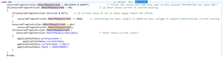
void ADC12_init(void)
{
    GPIO_setAsPeripheralModuleFunctionInputPin(GPIO_PORT_P6,GPIO_PIN0);
    GPIO_setAsPeripheralModuleFunctionInputPin(GPIO_PORT_P6,GPIO_PIN1);
    GPIO_setAsPeripheralModuleFunctionInputPin(GPIO_PORT_P6,GPIO_PIN2);
    GPIO_setAsPeripheralModuleFunctionInputPin(GPIO_PORT_P6,GPIO_PIN5);
    GPIO_setAsPeripheralModuleFunctionInputPin(GPIO_PORT_P6,GPIO_PIN6);
    GPIO_setAsPeripheralModuleFunctionInputPin(GPIO_PORT_P7,GPIO_PIN0);

    ADC12_A_configureMemoryParam CH0_configureMemoryParam = {0};
    ADC12_A_configureMemoryParam CH1_configureMemoryParam = {0};
    ADC12_A_configureMemoryParam CH2_configureMemoryParam = {0};
    ADC12_A_configureMemoryParam CH3_configureMemoryParam = {0};
    ADC12_A_configureMemoryParam CH4_configureMemoryParam = {0};
    ADC12_A_configureMemoryParam CH5_configureMemoryParam = {0};

    CH0_configureMemoryParam.memoryBufferControlIndex = ADC12_A_MEMORY_0;
    CH0_configureMemoryParam.inputSourceSelect = ADC12_A_INPUT_A0;
    CH0_configureMemoryParam.positiveRefVoltageSourceSelect = ADC12_A_VREFPOS_AVCC;
    CH0_configureMemoryParam.negativeRefVoltageSourceSelect = ADC12_A_VREFNEG_AVSS;
    CH0_configureMemoryParam.endOfSequence = ADC12_A_NOTENDOFSEQUENCE;

    CH1_configureMemoryParam.memoryBufferControlIndex = ADC12_A_MEMORY_1;
    CH1_configureMemoryParam.inputSourceSelect = ADC12_A_INPUT_A1;
    CH1_configureMemoryParam.positiveRefVoltageSourceSelect = ADC12_A_VREFPOS_AVCC;
    CH1_configureMemoryParam.negativeRefVoltageSourceSelect = ADC12_A_VREFNEG_AVSS;
    CH1_configureMemoryParam.endOfSequence = ADC12_A_NOTENDOFSEQUENCE;

    CH2_configureMemoryParam.memoryBufferControlIndex = ADC12_A_MEMORY_2;
    CH2_configureMemoryParam.inputSourceSelect = ADC12_A_INPUT_A2;
    CH2_configureMemoryParam.positiveRefVoltageSourceSelect = ADC12_A_VREFPOS_AVCC;
    CH2_configureMemoryParam.negativeRefVoltageSourceSelect = ADC12_A_VREFNEG_AVSS;
    CH2_configureMemoryParam.endOfSequence = ADC12_A_NOTENDOFSEQUENCE;

    CH3_configureMemoryParam.memoryBufferControlIndex = ADC12_A_MEMORY_5;
    CH3_configureMemoryParam.inputSourceSelect = ADC12_A_INPUT_A5;
    CH3_configureMemoryParam.positiveRefVoltageSourceSelect = ADC12_A_VREFPOS_AVCC;
    CH3_configureMemoryParam.negativeRefVoltageSourceSelect = ADC12_A_VREFNEG_AVSS;
    CH3_configureMemoryParam.endOfSequence = ADC12_A_NOTENDOFSEQUENCE;

    CH4_configureMemoryParam.memoryBufferControlIndex = ADC12_A_MEMORY_6;
    CH4_configureMemoryParam.inputSourceSelect = ADC12_A_INPUT_A6;
    CH4_configureMemoryParam.positiveRefVoltageSourceSelect = ADC12_A_VREFPOS_AVCC;
    CH4_configureMemoryParam.negativeRefVoltageSourceSelect = ADC12_A_VREFNEG_AVSS;
    CH4_configureMemoryParam.endOfSequence = ADC12_A_NOTENDOFSEQUENCE;

    CH5_configureMemoryParam.memoryBufferControlIndex = ADC12_A_MEMORY_12;
    CH5_configureMemoryParam.inputSourceSelect = ADC12_A_INPUT_A12;
    CH5_configureMemoryParam.positiveRefVoltageSourceSelect = ADC12_A_VREFPOS_AVCC;
    CH5_configureMemoryParam.negativeRefVoltageSourceSelect = ADC12_A_VREFNEG_AVSS;
    CH5_configureMemoryParam.endOfSequence = ADC12_A_NOTENDOFSEQUENCE;

    ADC12_A_init(ADC12_A_BASE,ADC12_A_SAMPLEHOLDSOURCE_SC,ADC12_A_CLOCKSOURCE_ACLK,ADC12_A_CLOCKDIVIDER_1);
    ADC12_A_setupSamplingTimer(ADC12_A_BASE,ADC12_A_CYCLEHOLD_256_CYCLES,ADC12_A_CYCLEHOLD_4_CYCLES,ADC12_A_MULTIPLESAMPLESENABLE);
    ADC12_A_setResolution(ADC12_A_BASE,ADC12_A_RESOLUTION_12BIT);

    ADC12_A_configureMemory(ADC12_A_BASE,&CH0_configureMemoryParam);
    ADC12_A_configureMemory(ADC12_A_BASE,&CH1_configureMemoryParam);
    ADC12_A_configureMemory(ADC12_A_BASE,&CH2_configureMemoryParam);
    ADC12_A_configureMemory(ADC12_A_BASE,&CH3_configureMemoryParam);
    ADC12_A_configureMemory(ADC12_A_BASE,&CH4_configureMemoryParam);
    ADC12_A_configureMemory(ADC12_A_BASE,&CH5_configureMemoryParam);

    /* VSENA */
    ADC12_A_clearInterrupt(ADC12_A_BASE,ADC12IFG0);
    ADC12_A_enableInterrupt(ADC12_A_BASE,ADC12IE0);

    /* VSENB */
    ADC12_A_clearInterrupt(ADC12_A_BASE,ADC12IFG1);
    ADC12_A_enableInterrupt(ADC12_A_BASE,ADC12IE1);

    /* VSENC */
    ADC12_A_clearInterrupt(ADC12_A_BASE,ADC12IFG2);
    ADC12_A_enableInterrupt(ADC12_A_BASE,ADC12IE2);

    /* VSENVM */
    ADC12_A_clearInterrupt(ADC12_A_BASE,ADC12IFG5);
    ADC12_A_enableInterrupt(ADC12_A_BASE,ADC12IE5);

    /* POT */
    ADC12_A_clearInterrupt(ADC12_A_BASE,ADC12IFG6);
    ADC12_A_enableInterrupt(ADC12_A_BASE,ADC12IE6);

    /* ISEN */
    ADC12_A_clearInterrupt(ADC12_A_BASE,ADC12IFG12);
    ADC12_A_enableInterrupt(ADC12_A_BASE,ADC12IE12);

    __enable_interrupt();

    ADC12_A_enable(ADC12_A_BASE);
    ADC12_A_startConversion(ADC12_A_BASE,
                            ADC12_A_MEMORY_0 |
                            ADC12_A_MEMORY_1 |
                            ADC12_A_MEMORY_2 |
                            ADC12_A_MEMORY_5 |
                            ADC12_A_MEMORY_6 |
                            ADC12_A_MEMORY_12, ADC12_A_REPEATED_SEQOFCHANNELS);
}
ADC interrupt
#pragma vector = ADC12_VECTOR
__interrupt void ADC12ISR (void)
{
    switch (__even_in_range(ADC12IV, 34))
    {
        case 0: break; //Vector 0: No interrupt
        case 2: break; //Vector 2: ADC overflow
        case 4: break; //Vector 4: ADC timing overflow
        case 6:
            phaseA = ADC12_A_getResults(ADC12_A_BASE,ADC12_A_MEMORY_0);
            break; //Vector 6: ADC12IFG0
        case 8:
            phaseB = ADC12_A_getResults(ADC12_A_BASE,ADC12_A_MEMORY_1);
            break; //Vector 8: ADC12IFG1
        case 10:
            phaseC = ADC12_A_getResults(ADC12_A_BASE,ADC12_A_MEMORY_2);
            break; //Vector 10: ADC12IFG2
        case 12:break; //Vector 12: ADC12IFG3
        case 14: break; //Vector 14: ADC12IFG4
        case 16:
            //vccSupplyVoltage = ADC12_A_getResults(ADC12_A_BASE,ADC12_A_MEMORY_5);
            vccSupplyVoltage = ADC12_A_getResults(ADC12_A_BASE,ADC12_A_MEMORY_5) * 0.014;
            break; //Vector 16: ADC12IFG5
        case 18:
            drvPOT = ADC12_A_getResults(ADC12_A_BASE,ADC12_A_MEMORY_6);

            if( POT_counter <= 5)
                POT_Toplam += ADC12_A_getResults(ADC12_A_BASE,ADC12_A_MEMORY_6);

            if( POT_counter == 5 )
                POT_Ortalama = POT_Toplam/5;

            if( POT_counter > 5 )
                POT_Ortalama = ( POT_Ortalama * 4 + ADC12_A_getResults(ADC12_A_BASE,ADC12_A_MEMORY_6)) / 5;

            if( POT_counter < 6)
                POT_counter++;

            //PWM = POT_Ortalama / 25.6;

            break; //Vector 18: ADC12IFG6
        case 20: break; //Vector 20: ADC12IFG7
        case 22: break; //Vector 22: ADC12IFG8
        case 24: break; //Vector 24: ADC12IFG9
        case 26: break; //Vector 26: ADC12IFG10
        case 28: break; //Vector 28: ADC12IFG11
        case 30:
            //drvISEN = ADC12_A_getResults(ADC12_A_BASE,ADC12_A_MEMORY_12);

            if( ISEN_counter <= 5)
                ISEN_Toplam += ADC12_A_getResults(ADC12_A_BASE,ADC12_A_MEMORY_12);

            if( ISEN_counter == 5 )
                ISEN_Ortalama = ISEN_Toplam/5;

            if( ISEN_counter > 5 )
                ISEN_Ortalama = ( ISEN_Ortalama * 4 + ADC12_A_getResults(ADC12_A_BASE,ADC12_A_MEMORY_12)) / 5;

            if( ISEN_counter < 6)
                ISEN_counter++;

            drvISEN = ISEN_Ortalama;

            break; //Vector 30: ADC12IFG12
        case 32: break; //Vector 32: ADC12IFG13
        case 34: break; //Vector 34: ADC12IFG14
        default: break;
    }
}
While the engine is running, the adc value on the compiler is constantly changing. When I measure the ISEN pin with a multimeter, the value appears to be 75mA.
What is wrong here?
Ali,