This thread has been locked.

If you have a related question, please click the "Ask a related question" button in the top right corner. The newly created question will be automatically linked to this question.

DRV8350: DRV8350 failure issues

Part Number: DRV8350

Dear, 

Over the last years we have used and designed a board with the DRV8350 gate driver for a light electric vehicle. Right now we are observing our first production series (200 boards, 800 DRV's) with fine results so far. 

As we are further developing the system -and spending more time on performance optimization- we are now experiencing two issues with the design involving the DRV8350S gate driver.

  1. During the rising edge of the high side FET we can observe the Vgs holding at 4.5v just as the SH node starts coming up. After this plateau we expect the gate voltage to keep rising with a similar dv/dt. Similarly during the rising edge of the low side FET we observe this as the SH node is coming down. It seems that after the plateau the gate driver is no longer sourcing current as is set in the IDRIVEP but instead is sourcing at the lowest rate which it does in the IHOLD state.
  2. The second issue has to do with the IDRIVE setting of the low side driver. The IDRIVE setting for the HS drivers is 300mA for P and 600mA for N. The IDRIVE setting for the LS drivers is 100mA for P and 200mA for N, increasing the IDRIVEN_LS to 300mA results in a VGLS/VCP error and a shorted out GLA pin. We then have to replace the driver due to the permanent damage.

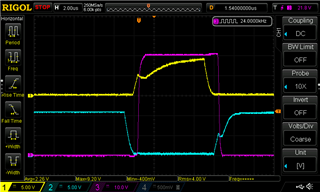
So essentially with low IDRIVE setting we are able to run the board very stable, but in the future we would like to get the mosfets to switch faster to increase performance. We are not sure if the two issues might be related to each other. But the image above shows a clear view of the first issue. (yellow being the high side Vgs, blue low side Vgs, purple Vds low side)

Some background information

A 48v DC motor is connected between phase A and phase B, the third phase is not being used. The SLC pin is tied to GND and SHC has a 10k resistor to GND. A 12vdc supply is connected to VM and Vdrain is powered with a 48v battery. The 1-PWM synchronous mode is used in this application which is set over SPI. INLC is tied high as braking is not used. INLA and INLB are set to low while driving INHB to high fixes the commutation to A-B, INHC toggles the direction of the current.
We've used the STH240N10F7-6 FET's in a H bridge setup and next to 4x1uF and 4x10uF ceramic decoupling caps a bank of 20x120uF electrolytic capacitors are the bulk. The PCB is a 2oz outer, 1.5oz inner 6-layer stackup. Due to high motor currents the power planes are 20mm wide, the gate driver is placed next to these planes, traces towards these planes are connected with net-ties to ensure proper routing.

Some help would be much appreciated, we have conducted quite some tests already but are not able to find the root cause of the issue our selves.

Kind Regards,

Willem

  • Hi Willem,

    Thanks for sharing results and background information so far. 

    It looks like the VGS waveform of the high side is charging a capacitive region slowly after the miller plateau is reached, which I agree, it should not turn on like this with respect to source since the dV/dt is much slower than before the miller plateau region. 

    • Does increasing the IDRIVE setting help on the high side driver? 
    • How long are the gate drive traces? Longer gate drive traces add more capacitance to the line. 
    • Does this happen all the time, or under certain conditions (i.e. motor loaded)?

    It may be good to look at the schematic and/or layout as well to see if we can pinpoint any issues.

    Thanks,
    Aaron

  • Hi Aaron,

    Thank you for your reply. Please find my answers below.

    • Increasing IDRIVE does not help with the described effect. The first slope is quicker as you may expect and some ringing starts which is not surprising. Please see the image below for a comparison of two IDRIVE settings for high side. (300mA compared to 100mA)

    • Gate traces are quite long indeed, longest trace is 85mm (Side A), shortest trace is 54mm (Side B). Please note that we do not see differences between the behavior for A or B. If trace lengths (inductance) would be the issue, wouldn't we also see the effect on the low side?
    • To clear a small mistake in my earlier explanation; the 'normal operation' is with a 48V motor connected, but in our experiments to find the issue we disconnected the motor. So all traces that you see in the scope plots are WITHOUT anything connected.

    Schematics are mostly according to the TI reference design. Attached a screenshot of one of the gate lines to High Side B. For sharing more details, is a private (e-mail) possible?

    We have some bulk caps between DRV and H-bridge due to power routing choices we made.

    Cheers,

    Willem

  • Hi Willem,

    We have looked into this further and have the following feedback:

    Alignment items:

    • Regarding the schematic and layout files, can you help share them to me at andrew.liu@ti.com ? 
      • what software tool are you using for the schematic and layout capture? Altium/Allegro-Cadence/Gerber is preferred,
        but the files are essential for us to help debug this further 
    • Just wanted to confirm - when you say that you are experiencing VGLS/VCP error when increasing LS IDRIVE to 300mA, is this showing up as a confirmed nFAULT flag & is it reporting as such in the SPI fault registers for these two undervoltage protections?
    • For the first problem reported above about Vgs waveforms, does this same problem occur for all 3 output phases? (A,B,C)
    • Waveform capture requested: 
      • VCP pin, VGLS pin, HS FET Vgs (measured between GHx and SHx), LS FET Vgs (measured between GLx and SLx)

    Some thoughts on the debug: 

    1. for the first problem reported about the slew rate of the Vgs waveforms on both HS and LS,
      1. our main suspicion is that there are parasitics in the system causing that behavior
      2. this could be from many sources, such as: 
        1. gate drive trace and thickness, interfering with the ability of the DRV device to drive the gates optimally 
        2. component placement, voltage ratings, and routing for the caps related to VGLS, VCP, VM, CPH/L, etc..
        3. other general items for system grounding and current-carrying paths 
      3. reviewing the schematic and layout will allow for us to look for possible root causes 

    2. for the second problem of LS IDRIVE setting limitation to avoid damage, 
      1. the VGLS cap and other DRV-related caps could be impacting this as well, especially if they are placed far from the DRV IC or have their effective capacitance impacted by voltage de-rating or non-ideal PCB routing 
      2. We are a bit curious as to the exact failure mechanism of damage to the device's gate-drivers at 300mA IDRIVE operation, so that's why some waveform captures were requested above to better understand this behavior 
      3. reviewing the schematic + layout in this case may be helpful as well 

    Thanks and Best Regards,
    Andrew

  • Hi Willem, 

    Following up on this e2e post - please let us know if you need additional support from us on this debug.

    Did the information provided below resolve your problem?

    Thanks and Best Regards,

    Andrew 

  • Hi Andrew,

    We have not resolved it yet. Today we did some experiments with different wire lengths/thickness from DRV to mosfets. We are still collecting the data and images and will send you a report later.

    Thanks for your patients.

    Kind Regards,

    Willem

  • Hi Willem,

    Understood, and thanks for the update on this - 

    To help streamline the scope of the trace thickness aspect of the gate drive trace validation, I would make a quick mention that we recommend 15-20 mils for most applications. Some other top-priority considerations for gate drive traces are:

    1. have each phase's channel be similar in length to one another
    2. avoid right-angle traces. add teardrops where possible to keep the signal path more consistent 
    3. make sure to handle the grounding scheme properly -
      1. if you have a split ground between DRV device and MOSFET power stage, want to have low inductance net tie near the DRV device 

    I've also attached some resource links below, in case your team 

    https://www.ti.com/lit/an/slva959b/slva959b.pdf (Board Layout) 

    https://www.ti.com/lit/an/slvaf66/slvaf66.pdf (High-power system design) 

    Thanks and Best regards,
    Andrew 

  • Hi Willem,

    Has your issue been resolved?

    Thanks,
    Aaron

  • Hi Willem, 

    Following up on this e2e discussion, do you require any additional assistance on this debug effort? 

    Best Regards,
    Andrew

  • Hi Andrew,

    The issue is still there, we did collect more information and data and will send you an e-mail straight away.

    Kind Regards,

    Willem Zwetsloot

  • Hi Willem,

    Thanks for the follow-up, and will follow up on this via email. I may need a bit more time than usual to give some more feedback on this, since I have to take care of quite a few lab-related activities due this week 

    Thanks and Best Regards,
    Andrew

  • Hi Willem, 

    Sent over some comments via email on the sch/layout documents. 

    Latest speculation is that the extra 1uF capacitor between VCP pin and GND is not part of the datasheet recommendation, and might explain why VCP/VGLS UVLO errors occur when trying to increase IDRIVE current past a certain threshold. In cases where IDRIVE setting is sufficiently low to not trigger the nFAULT flags, this could still explain the dV/dt being quite low after reaching the miller voltage 

    Please try depopulating the capacitor, and then let us know if the problem(s) go away

    Thanks and Best Regards,
    Andrew