This thread has been locked.

If you have a related question, please click the "Ask a related question" button in the top right corner. The newly created question will be automatically linked to this question.

DRV8711EVM: High-side gate drive voltage range exceeding MOSFET maximum Vgs

Part Number: DRV8711EVM
Other Parts Discussed in Thread: DRV8711, CSD18531Q5A,

The high-side gate drive pin voltage (A1HS, A2HS, B1HS, B2H) in the DRV8711 datasheet is spec'd to range from -0.6V to VM+12V (see below).


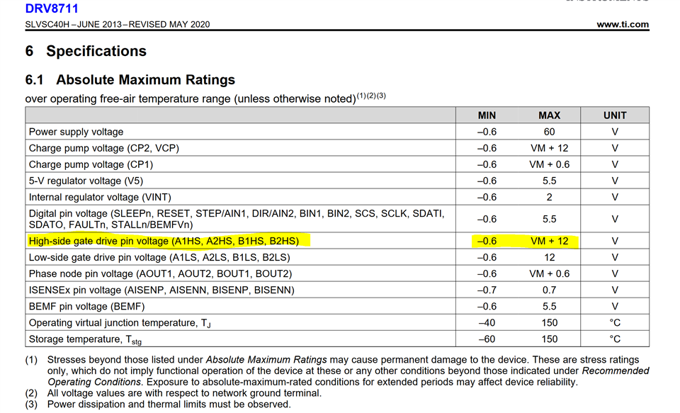
In simulations we have run we noted that before the driver starts generating output pulses there is a situation that appears to put the MOSFETs out of spec. Specifically, with VM => 40V (our system is 48V), it is possible the source of the high side MOSFET will be at 20V or greater (i.e. 1/2 * VM, or 24V in our system) - in this situation if the gate drive voltage is 0V (or down to -0.6V as the DRV8711 spec sheet says), the Vgs on the high side MOSFET will exceed -20V (-24V in our system) (see below).


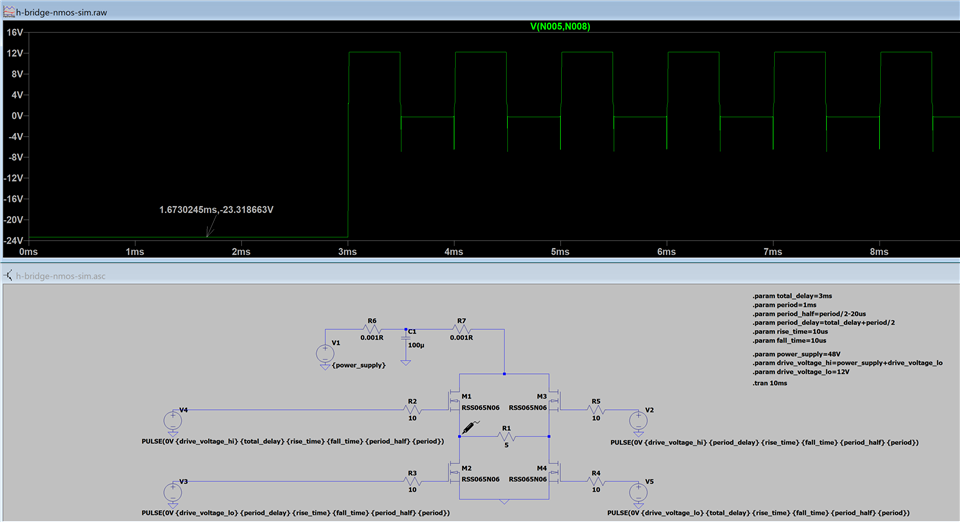
Most MOSFETs on the market have a maximum Vgs of +/-20V, which means with VM > 40V most MOSFETS would be out of spec with a 0V gate drive voltage. Specifically in the evaluation board, DRV8711EVM, the MOSFETs are CSD18531Q5A, which has a maximum Vgs of +/-20V (see below).


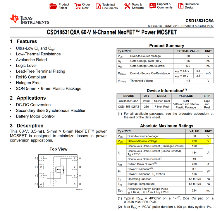
The eval baord suggested VM could be as high as 52V, but if this is the case and the high-side gate drive voltage is 0V, these MOSFETs are out of spec. I need to understand the characteristics of the high-side gate drive pin voltage in this chip and specifically must be able to definitively say that the MOSFETs maximum Vgs of +/-20v will not be exceeded. Can anyone provide test data or theory of operation that can assure me these high-side MOSFETs will stay in spec during operation?

  • Hi Nicholas,

    Thanks for posting to the forum. I'll be assisting you in resolving this issue. Please allow me 24 hours to analyze the information you provided.

    Thanks in advance for your patience.

  • Hi Pablo - how is this topic progressing? Do you need any more information?

  • Hi Nicholas,

    Have you tested this on real hardware or just in simulations? Simulations are helpful for understanding how the device will behave but may not be useful for providing real world data.

  • I was hoping to have some light shed on the output behavior of the high side drive before investing in a evaluation kit that I am concerned will blow the MOSFETs when tested under our systems conditions. Is there no one at TI who can provide a better description of this parts functionality?
    Simulations aside, it simply comes down to the question "is the high side output pin ever going to be held low?" - if the answer is yes, then the MOSFETs will be out of spec.

  • Hi Nicholas,

    "is the high side output pin ever going to be held low?" - if the answer is yes, then the MOSFETs will be out of spec.

    The xHS pins will be LOW when the control signal is LOW. Also, for the duration of the dead time, all outputs will be LOW. When all the FETs are disabled, any current in the motor will flow through the body diodes to VM. The FETs will have a VDS roughly equal to the forward voltage drop of the internal body diodes. The xHS is internally shorted to the corresponding xOUTx pins when the FETs are disabled. So there shouldn't be any worries about violating the VGS of the external FETs.

    I hope this answers your questions.