Other Parts Discussed in Thread: DRV832X
Hello team,
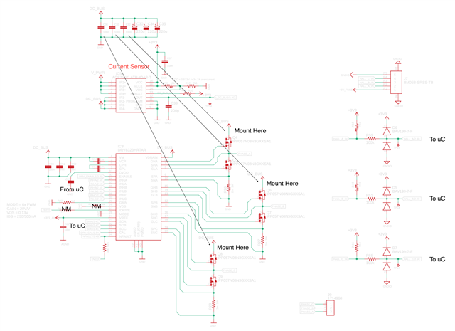
I am using the DRV8323HRTAR (no SPI) to drive a BLDC motor.
While the motor spins, it makes a strange rattling noise and I am trying to solve this issue.
I have implemented a trapezoidal upper modulation control with speed retroaction.
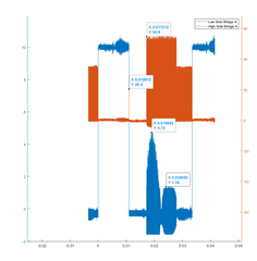
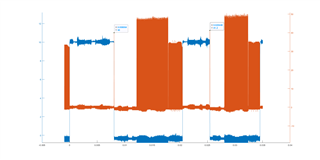
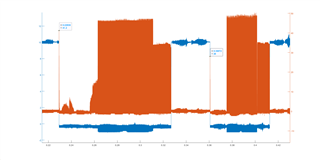
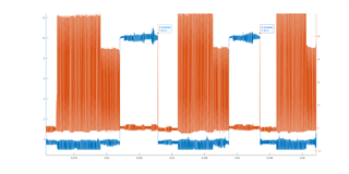
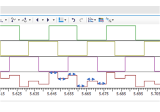
Analyzing some data (2-ch scope and CAN at 1ms cycle time) I am noticing that:
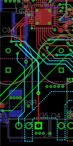
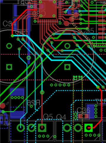
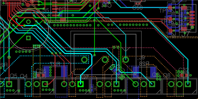
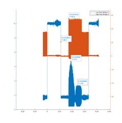
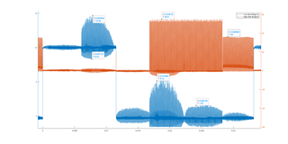
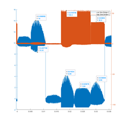
- Bridge A is behaving differently than B and C
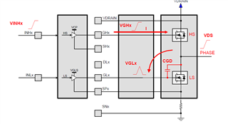
- Every time I turn off a low side mosfet, there is a voltage spike on the high side voltage gate
- While the high side mosfet is on, also the low side is on
CAN Data:
SOx = current measured via the shunt resistor by the DRV
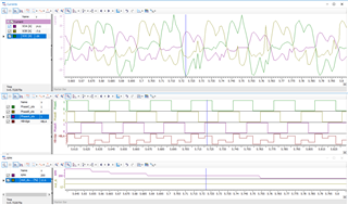
Scope Data:
- All the waveforms are the gate voltage measured with reference to ground
The DRV is configured as follow:
- GAIN = 20V/V
- MODE = 6x PWM
- IDRIVE = 120/240mA
- VDS = 0.6V
- Shunt = 2mohm
- No fault triggered by the NFAULT pin
Please let me know if you need any additional information.
Thank you
Simone Palombi