Hi,
I'm evaluating "DRV8308" now.
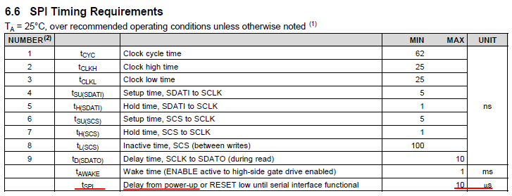
In the attached figure, "tAWAKE" is specified as 1ms (max) as the one of timing requiremet of SPI.
Does this mean that the ENABLE signal must be set to "H"(ENPOL=0) 1ms before the SPI read and write?
Best regards.
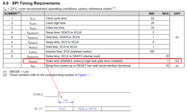
Hi,
I'm evaluating "DRV8308" now.
In the attached figure, "tAWAKE" is specified as 1ms (max) as the one of timing requiremet of SPI.
Does this mean that the ENABLE signal must be set to "H"(ENPOL=0) 1ms before the SPI read and write?
Best regards.