This thread has been locked.
If you have a related question, please click the "Ask a related question" button in the top right corner. The newly created question will be automatically linked to this question.
Hi team,
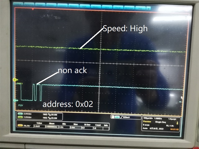
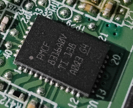
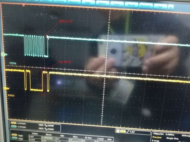
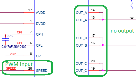
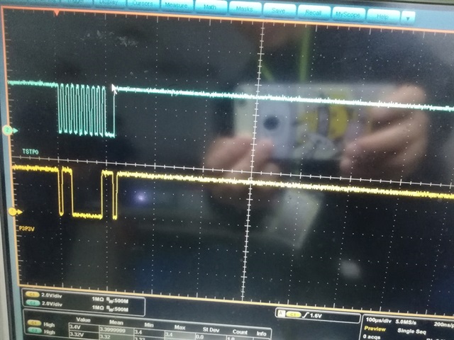
When the customer debugs the MCF8316A, it is found that the I2C always returns -7, and the measured I2C waveform is detailed in the attachment.
Configure as follows:
1) I2C: 0x60
2) data length: 32bit
3) CRC: No
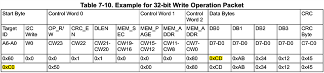
Programming logic: According to the format of Table 7-10, the data of each EEPROM address (take 0x00000080 address as an example) is as follows:
address 0x00000080 data is 0xC0, 0x10, 0x00, 0x80, 0x20, 0x8C, 0x63, 0x44 Every time you write an address corresponding to 8 bytes of data, it will delay 100ms
Excuse me, is the programming logic correct? If it is not correct, how to modify it?
Hi Jason,
We will look into this and aim to provide a response by early next week
Best Regards,
Andrew
Hi Andrew,
Customer has scheduled for the solution of replacement PMD1000, please help asap, thanks.
Customer confirm that DDP can not write data to MCF8316A with the function of I2C_MasterWrite or I2C_PolledMasterWrite.
The attached file is the driver for MCF8316A.
Could you please confirm if the driver is OK?
Jason
Hi Jason,
Could you please confirm whether the customer is using the RTM or APL version of the MCF8316A?
It looks like they are referencing the APL version of the datasheet, so if they switched over to using an RTM device, they would need to change the slave address to 0x01 according to the latest datasheet:
Regards,
Eric C.
Hi Eric,
Change address to "0x02", DDP can not write data to EEPROM of MCF8316A via I2C(always show non-ack in 9th clk, please see the attached picture).
How to confirm if MCF8316A is in sleep mode? If in sleep mode, how to wake up from sleep mode?
Jason
Hi Jason,
We can aim to provide a follow-up response early next week from Eric.
In the meantime, wanted to drop in one quick comment regarding the SLEEP mode configuration
Best Regards,
Andrew
Hi Andrew,
Thanks for your comments.
Update my customer questions.
Configure SPEED pin to control with PWM and set High for SPEED while data is wrote to EEPROM of MCF8316A.
I2C always show non-ack, please see the attched picture for address 0xC0/0x02.
Any settings need confirm or any solutions to resolve this phenomenon?
Jason
Hi Jason,
Could you please help confirm the following information with the customer so we can better support the issue:
Assuming the customer did not reprogrammed the EEPROM of the device (since they're getting NACKs), the factory default setting on the MCF8316A configures DEV_MODE = 0b (standby mode). This means the device will NOT enter SLEEP mode even if the SPEED pin is 0V. In fact, the customer should set the SPEED pin to 0V on power-up to prevent the MCF8316A from attempting to spin the motor immediately.
After they power up the device, could you please ask them to measure the following regulator output to ensure they are powered up properly:
Thanks,
Eric C.
HI Eric,
Please see below comments from customer.
Is the customer using the MCT8316A EVM or their own board design?
--> Our own board design
If this is on their own PCB, could you please share the schematic?
--> Please see the attached schematic(Replace PMD1000 SCHEMATIC_Core.pdf)
Could they please take a picture of the device package marking so that we can confirm whether they are using the RTM or APL device?
--> Please see the attached picture(MCF8316A picture.png)
What I2C clock frequency is the customer using?
--> I2C clk frequency is 100kHz
If possible, do they have a logic analyzer for capturing the I2C SDA/SCL? It would be much easier to decode the I2C communication.
--> We measured by oscilloscope, please see the attached picture(no ack with 0x02 address.jpg and no ack with 0xC0 address.jpg)
Buck regulator voltage Vbk output (BUCK_SEL = 01b, 5V by default)
--> 1.1918V
AVDD (3.3V)
--> 3.28V
DVDD (1.5V)
--> 1.37V
Replace PMD1000 SCHEMATIC_Core.pdf
Jason
Hi Jason,
The customer is using a APL version of the MCF8316A, so the original 0x60 should be used as the default I2C slave address.
Vbk output of 1.19V indicates that the buck regulator is not configured correctly. Vbk should range from 3.3 to 5.7V.
Looking at the schematic, L8 inductor is not populated (NC) and R472 is 0Ω. If using resistor mode, R472 needs to be 22Ω in order for the buck regulator to be functional.
Please refer to table 7-1 in the datasheet for recommended settings for the buck regulator:
The internal circuitry in MCF8316A is powered from the buck regulator output, so please ask the customer to ensure that the buck regulator is configured correctly and outputting nominal voltage before attempting to communicate with the device via I2C.
Regards,
Eric C.
Hi Eric,
update customer questions, please see below.
Data(follow Table8.3 and config SPEED "PWM Input") can be wrote via I2C, but CW still can not work.
SPEED pin can measure PWM waveform, but OUT_A/B/C no output.
Do you have data of EEPROM similar to our hardware design or followed our hardware design?
Jason
Hi Jason,
Could you please ask the customer to follow the Essential Controls section in the MCF8316A Tuning Guide to configure the device to spin up the motor?
The motor parameters R, L, and Ke need to be either entered or measured using the device's built in MPET algorithm in order for the FOC algorithm to operate properly.
If the device still fails to drive OUT_A/B/C properly, the device might be hitting a fault condition. They can read back the GATE_DRIVER_FAULT_STATUS and CONTROLLER_FAULT_STATUS registers to find out what fault is triggering when attempting to spin up the motor.
Regards,
Eric C.
Hi Vishnu,
Update customer question, thanks.
1. CW can not work
2. Out A/B/C output wrong waveform (see the attached picture)
3. Address is 0xC0, configuration data (see the attached txt file)
4. When is available for our AE to have a con-call with customer?
/********************** I2C data word format ******************************/ /* Target_ID R/W Control_Word Data CRC_8 */ /* A6~A0 W0 CW23~CW0 D15/D31/D63~D0(LSB first) C7~C0 */ /***********************************************************************/ /********************** 24-bit control word format *****************************/ /* CW23 CW22 CW21~CW20 CW19~CW16 CW15~CW12 CW11~CW0 */ /* OP_R/W CRC_EN DLEN MEM_SEC MEM_PAGE MEM_ADDR */ /* 1: R 1: enable 00: 16bit 4bit 4bit 12bit */ /* 0: W 0: disable 01: 32bit */ /* 10: 64bit */ /* 11: reserve */ /*************************************************************************/ static DataFormat_32bit gRegisterAddressTable[RegisterMax] = { //Control Data+Address+Data(4 Bytes) {0x10, 0x00, 0x80, 0x20, 0x8C, 0x63, 0x44}, // 0x80 : init speed detect config {0x10, 0x00, 0x82, 0x64, 0xF0, 0x3A, 0x28}, // 0x82 : reverse driver config {0x10, 0x00, 0x84, 0xD0, 0x07, 0x68, 0x0B}, // 0x84 : motor start setting1 {0x10, 0x00, 0x86, 0x00, 0x60, 0x06, 0x23}, // 0x86 : motor start setting2 {0x10, 0x00, 0x88, 0xB0, 0x81, 0x31, 0x0C}, // 0x88 : close loop setting1 {0x10, 0x00, 0x8A, 0x00, 0x00, 0xAD, 0x1A}, // 0x8A : close loop setting2 {0x10, 0x00, 0x8C, 0x00, 0x00, 0x00, 0x00}, // 0x8C : close loop setting3 {0x10, 0x00, 0x8E, 0x2C, 0x01, 0x00, 0x00}, // 0x8E : close loop setting4 {0x10, 0x00, 0x90, 0x06, 0x02, 0xE8, 0x5F}, // 0x90 : config fault setting1 {0x10, 0x00, 0x92, 0x00, 0x00, 0x00, 0x74}, // 0x92 : config fault setting2 {0x10, 0x00, 0x94, 0x00, 0x00, 0x00, 0x00}, // 0x94 : config speed profile1 {0x10, 0x00, 0x96, 0x00, 0x00, 0x00, 0x00}, // 0x96 : config speed profile2 {0x10, 0x00, 0x98, 0x00, 0x00, 0x00, 0x00}, // 0x98 : config speed profile3 {0x10, 0x00, 0x9A, 0x00, 0x00, 0x00, 0x00}, // 0x9A : config speed profile4 {0x10, 0x00, 0x9C, 0x00, 0x00, 0x00, 0x00}, // 0x9C : config speed profile5 {0x10, 0x00, 0x9E, 0x00, 0x00, 0x00, 0x00}, // 0x9E : config speed profile6 {0x10, 0x00, 0xA0, 0x7D, 0x40, 0xB3, 0x00}, // 0xA0 : config init algo setting1 {0x10, 0x00, 0xA2, 0xA7, 0x01, 0x00, 0x00}, // 0xA2 : config init algo setting2 {0x10, 0x00, 0xA4, 0x00, 0x00, 0x00, 0x00}, // 0xA4 : config hardware pin {0x10, 0x00, 0xA6, 0x00, 0x00, 0x00, 0x00}, // 0xA6 : config device1 {0x10, 0x00, 0xA8, 0x00, 0xB0, 0x00, 0x00}, // 0xA6 : config device2 ----crystal OS {0x10, 0x00, 0xAA, 0x00, 0x00, 0x00, 0x40}, // 0xAA : config peri {0x10, 0x00, 0xAC, 0x00, 0x01, 0x00, 0x00}, // 0xAC : config gated driver setting1 {0x10, 0x00, 0xAE, 0x00, 0x00, 0x20, 0x00}, // 0xAE : config gated driver setting2 {0x10, 0x00, 0xEA, 0x00, 0x00, 0x50, 0x8A}, // 0xEA : config algo //{0x10, 0x00, 0xEA, 0x00, 0x00, 0x00, 0x00}, // 0xEA : config algo };
Jason
Hi Jason,
As discussed in email, we'll continue to support this issue offline and on the scheduled call.
We may need to simply ask the customer to load in the pre-configured register settings first before spinning up the CW.
Regards,
Eric C.