This thread has been locked.

If you have a related question, please click the "Ask a related question" button in the top right corner. The newly created question will be automatically linked to this question.

DRV8323: Current Sense amplifier unused, Device GND or Mosfet Source

Part Number: DRV8323

E2E:

We currently use the DRV8320SRTV in our brushless motor controller with a single external current sense amplifier. For availability reasons, we're designing in the RV8323SRTA, but we do not intend on using its internal amplifiers. We are keeping our single external amplifier to mitigate risk.

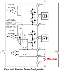
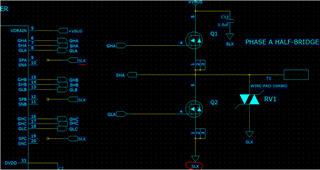
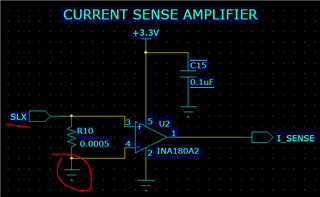
The 8323's amplifiers pins replace the SLx pins that we use on the 8320, and it is a bit ambiguous in the datasheet, for our specific application, where we need to connect the SPx and SNx pins for each amplifier if we want to run the 8323 as if it were our original 8320. The relevant portion of the schematic is below:

As noted here: https://e2e.ti.com/support/motor-drivers-group/motor-drivers/f/motor-drivers-forum/676345/drv8323-current-sense-amplifier-question

They are told to connect the unused amplifier inputs to GND.

Where would be the best place to connect the SPx and SNx pins? 


Thank you!

  • Hey Marcos,

    I will aim to provide a feedback later next week. 

    Best Regards,

    Akshay

  • The ambiguity of what to do with the current sense amplifiers comes from the different recommendations given on E2E and what is on the data sheet.

    From the data sheet:


    Screenshot 1.

    Screenshot 2.

    Screenshot 3.


    I have taken 3 screenshots from the relevant sections in the datasheets:

    In SC 1. I interpret it as only the SPx pins are connected to the low-side FET source. 

    In SC 2. it would seem to reinforce the idea of connecting the SP pins to the low-side FET source but also suggest that both the SPx and SNx pins should be connected to the low-side FET source.

    In SC 3. it says to connect the SPx and SNx pins to the low-side FET source if they are not used.

    None of these configurations describes the specific configuration of having a single current sense resistor at the low-side FET source for all 3 phases. 


    DRV8323: Current Sense amplifier question - Motor drivers forum

    In this response about not using the current sense amplifier where they are using an external sensing scheme, the advice given was to connect the SPx and SNx pins to GND. Is this the device GND or the low-side FET source? Basically before or after the current sense resistor.

    DRV8323: best practices for unused current sense amplifiers - Motor drivers forum

    In this response to using a single shunt design it was also recommended to connect the SPx and SNx pins to GND. In the response clarification it is recommended to connect the unused ADC pins to the GND side of the resistor.

  • Hey Marcos,


    Thank you for your patience.


    The inputs of the CSA, SPx and SNx, can be tied together and connected to GND. This is to ensure that the CSA won’t operate and have fluctuations on SOx.


    You can float the CSA output, SOx, to prevent current wastage.


    Best Regards,

    Akshay

  • Akshay,


    If we connect the CSA inputs to GND, would that mean we need to adjust the overcurrent threshold to account of the voltage drop for the current sense resistor? The new equivalent Rdson will include the current sense resistor.


    If we connect the CSA inputs to the low-side FET source we would not need to adjust the Overcurrent threshold from the previous design. The SPx and SNx will be tied together at the pins of the microcontroller. Would this not ensure that there is no voltage difference between the pins so that the SOx does not operate or fluctuate?


    Thank you,
    Marcos L

  • If we connect the CSA inputs to the low-side FET source we would not need to adjust the Overcurrent threshold from the previous design. The SPx and SNx will be tied together at the pins of the microcontroller. Would this not ensure that there is no voltage difference between the pins so that the SOx does not operate or fluctuate?

    Yes, but the overcurrent threshold you're referring to would be the VSEN overcurrent threshold.

    VDS_OCP will still operate as normal.

    Best Regards,

    Akshay

  • TI will need to confirm, however, Figure 41 from the datasheet tells a good story for how this works internally. Since for Vds monitoring you're going to want to measure the rdson of the low side FET as the best you can, you'll want your connection to be close to the source (not GND). Then to make the output of the amplifier stay low, you can tie the two together.

    However you'll need to be careful to stay within spec of the amplifier to prevent any damage. For this you'll care about the common mode voltage range. The datasheet doesn't list a max, but as long as you stay within the operating range it should be fine.

    - Will

  • Hey Marcos,

    If you use the internal CSA then you wouldn't want the CSA inputs to vary by more than Vcom, as exceeding them means you will not be in linear region of the CSA. But if you are not using them then there is no concern.

    Best Regards,

    Akshay

  • The CSA max voltage would be -1 to 1 V. 


    Thank you,

    Marcos L