


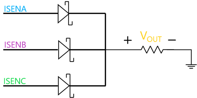
When it comes to designing your system, sometimes you may find that there is a limited amount of ADC channels available on your MCU. One way that you can reduce the number of needed ADC channels is by converting the 3 CSA outputs from your BLDC Integrated FET device into one (Please keep in mind that this implementation is intended to be used by trapezoidal commutation as FOC/sinusoidal may require the output from all 3 CSAs).
One method to convert the outputs of 3 CSAs into one involves the usage of 3 Schottky diodes. To do this, you will need to follow these steps:
- Connect each of the outputs of the CSAs to the anode of a Schottky diode and connect their cathodes together to create a combined output voltage.
- Connect a load resistor across the combined output voltage to convert the current measurement into a voltage measurement that can be read by a voltage measurement circuit.
- Make sure that the load resistor is able to pull-down the current fairly quickly. The recommended range for load resistors is between 10KΩ-100KΩ.
NOTE: Do not forget to account for the diode voltage drop from the CSA output to the ADC
The circuit diagram for the above steps is shown in the image below:
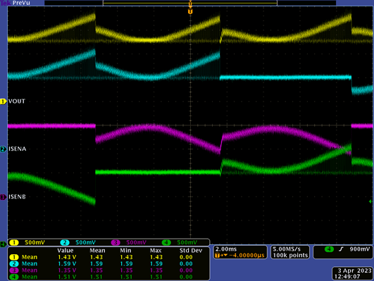
The waveforms below showcase traces monitoring the voltage across VOUT as well as the ISENA, ISENB, and ISENC pins using the DRV8311HEVM with the following configurations:
- PVDD = 15 V
- GAIN = 2 V/A
- SLEW = 200 V/μs
- MODE = 6x PWM mode
- Load Resistor = 20KΩ
Waveform 1: 10% duty cycle
Waveform 2: 50% duty cycle
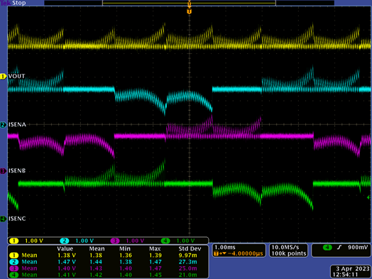
Waveform 3: 90% duty cycle

