This thread has been locked.

If you have a related question, please click the "Ask a related question" button in the top right corner. The newly created question will be automatically linked to this question.

DRV8711: Damaged DRV8711 - overcurrent

Part Number: DRV8711
Other Parts Discussed in Thread: CSD88537ND,

Hi,

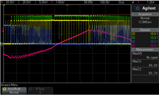
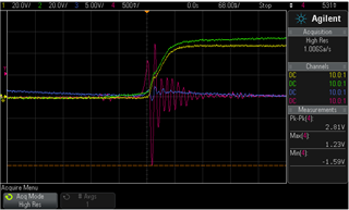
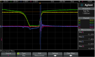
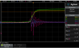
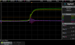
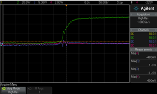
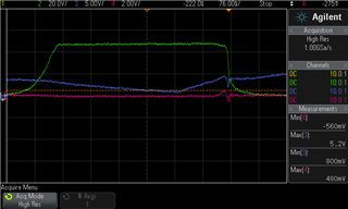
We have issues with the DRV8711 where in some cases it gets damaged: once current regulation is enabled (CTRL.ENABLE=1) an overcurrent error is triggered. Lowering current setpoint (CTRL.ISGAIN, TORQUE) or increasing OCP settings (DRIVE.OCPTH, DRIVE.OCPDEG) does not help. We have to replace the DRV8711 IC to fix the issue so it seems that the IC gets damaged. It also happens when starting motion (pulses at STEP input). In some cases a predriver fault is triggered.

We use different decay modes for standstill and motion, mostly to lower standstill noise.

It is hard to reproduce the issue at our department: it happens now and then at customers.

Our design:

Steppermotor NEMA 17: bipolair, 1.5 A/phase, 2.4 Ohm/phase, 2.6 mH/phase

Drivervoltage/VM: 48V

FETs: TI CSD88537ND

Rsense: 0.05Ohm

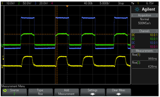
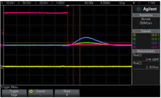
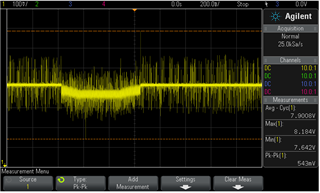
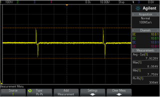
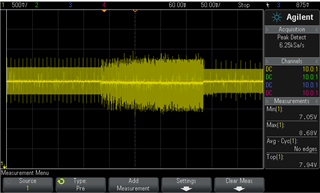
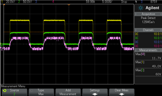
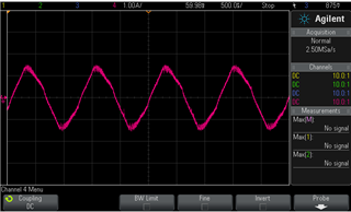
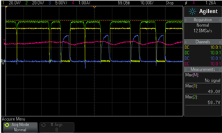
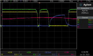
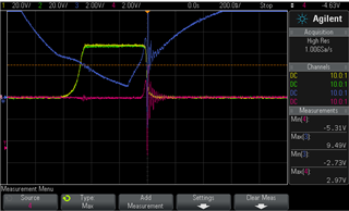
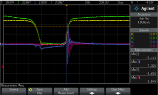
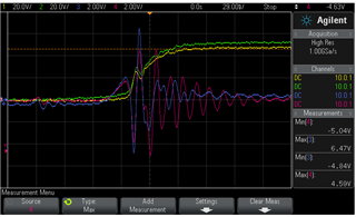
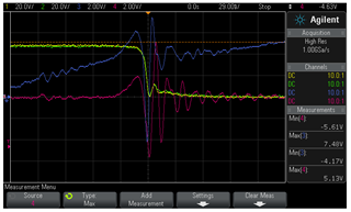
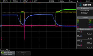
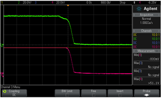
We've optimized DRV8711 settings based on audible noise and smoothness of the current curve (measuring FET output current on scope):

DRV8711 motor hold (standstill) settings:

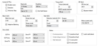
DRV8711 motor run settings (max : 53000 steps/s)

Equal to the above, except:

  • Decay mode: mixed
  • Blank time: 2.0µs
  • Off time: 4 µs

Can you explain what happened to the damaged DRV8711? Can it be a temperature issue?

  • Hi Tijmen,

    I would try to do the following for a start:

    - increase DriveTN and DriveTP times

    - try to find settings that would work both for run and stanstill so it would not be necessary to change them, I think auto mixed decay mode is worth of trying

    - check if VM stays around 48V all the time (it may increase significantly in case of breaking and resonances),

    - check if PCB layout is made according to Layout Guidelines.

    Regards,

    Grzegorz

  • Hi Tijmen,

    Please give me 2 hours to look into your questions. I will get back with a reply as soon as possible.

    Regards,

    Pablo Armet

  • Hi Mr Pelikan,

    Thank you for your suggestions. 

    Tijmen,

    I supported another customer with a very similar issues that you are experiencing. In their case, increasing TDRIVE help prevent the OCP and pre-driver faults. Can you set TDRIVE to the max value and run your motor.

    Regards,

    Pablo Armet

  • Hello Pablo,

    Thanks for your feedback.

    We will get back to you on 16th of May.

    Kind regards,

    Guido Vermeulen (colleague of Tijmen)

  • Hello Grzegorz,

    Thank you! I will check 48V while running and stopping the motor.

    What would be the effect of increasing DriveTN and DriveTP and how will it help preventing DRV8711 getting damaged? Is it possible to provide some background on your suggestion?

  • Hello Pablo,

    Thank you for your suggestion.

    I supported another customer with a very similar issues that you are experiencing.

    Can I find this case on the E2E forum?

    Can you set TDRIVE to the max value and run your motor.

    I can do that. How will it help preventing DRV8711 getting damaged? Is it possible to provide a background? (i've read SLVA714A: understanding IDRIVE and TDRIVE).

    Thanks!

    Tijmen

  • Hi Tijmen,

    Looking at your IDRIVE settings and Mosfet gate charges and comparing them to mine I guess your output voltage rise/fall times are somewhere around 80ns. It is time necessary to charge Qgd but to charge fully Mosfet gate (Qg) we need time several times longer. TDRIVE time of 250ns may not be long enough to fully charge Mosfet gates in your design. In this case Mosfet RdsOn may be much higher than it should be and you would get higher mosfet power losses and OCP faults. I am not sure If this can lead to DRV8711 damage but it should be avoided. As Pablo suggested you can increase TDRIVE to its max value, this way you will get a good safety margin.

    It is just one of possible causes of DRV8711 failure but problem can be something else. I think your IDRIVE settings should be OK for your Mosfets and you should not increase them.

    RL time constant of your motor is quite low, you may try to lower Toff time (50us) a bit.

    Unfortunately, usually finding a failure cause is not easy and eliminating all possible/potential issues may be a good way to solve the problem.

    Regards,

    Grzegorz

  • Hi Grzegroz,

    Thanks for your reply. We are running tests with TdriveP/N set to maximum and other optimizations on current decay settings. Unfortunately, the issue happens once in a while (at a customer) so it is hard to draw conclusions yet.

    Do you have any suggestions what to measure to get to the bottom of this issue? We already measured VM on a good DRV8711 and observed a slight drop in voltage (~1 Volt) when the motor was running. No spikes found.

  • Hi Tijmen,

    I think the most probable cause of your problems is exceeding max. absolute voltage rating of some pin/pins caused by voltage over/undershoot, ringing

    or motor breaking.

    I would do the following:

    check if PCB layout is made according to Layout Guidelines

    - check if by a chance motor is not driving vertical axis with a weight that can cause regenerative braking and VM voltage spike

    - check xOUTx, xLS, xHS, xISENx pins with an oscilloscope for any voltage spikes/ ringing, up to around 100 MHz or even higher

    - try to drive a bigger motor like NEMA 23 with current around 2-2,5 times higher several times for a couple of seconds and see if board survives

    - try to add around 100 Ohm LS gate resistors and see if it helps

    - try to find settings that would work both for run and stanstill so it would not be necessary to change them

    - check if customer have possibility to change anything that could lead to driver failure

    - check DRV8711 temperature

    - check environment that your boards operate in ie. high temperature, humidity, long cables connected to pcb + strong electromagnetic fields etc.

    - try to notice conditions when failure happens like speed, acceleration phase, is there a chance of motor cable failure if the cable is under mechanical stress?

    I guess it may be quite difficult to find a cause of the issue because failure does not happen often and anything you change you will have to wait some time to verify if it helps or not.

    Regards,

    Grzegorz

  • Hi,

    Monday 29th is national holiday in US. Please expect our response later on Tuesday.

    regards

    Shinya 

  • Hello Tijmen,

    Gregory suggestions are great for debugging. Have you been able to test them?

    Regards,

    Pablo Armet

  • Hi Pablo,

    Not yet, we're testing increased Tdrive times + skip switching decay modes first. The design is very compact (and contains 2x DRV8711 drivers) so we need to discuss how to probe xOUTx, xLS, xHS, xISENx.

    The design already has a 240 Ohm gate resistor for both LS and HS.

    It is a vertical axis (Z) so there is regenerative braking involved.

    Driving a NEMA23 motor will be the next step.

    Kind regards,

    Tijmen

  • Hi Tijmen,

    Thank you for the update. Let me know if you need further support with your debugging.

    Regards,

    Pablo Armet

  • try to drive a bigger motor like NEMA 23 with current around 2-2,5 times higher several times for a couple of seconds and see if board survives

    The board survives repeated motions of a NEMA 23 motor running at 4.0 A, accelerating from 80-600 mm/s in 150 ms. Surface temperature of the IC peaks at ~60°C.

    The PCB of the customer has arrived and it reports a B overcurrent error once motion is started (using the settings listed in my first post). However, when increasing DriveTP/TN to 2µs the OCP fault does not occur, even during repeated, fast (de)accelerating motions.

    We're gonna attach some wiring to monitor gate driver inputs/outputs, both to a healty (undamaged) driver and the (damaged?) driver returned by the customer.

  • Hi Tijmen,

    Thank you for your answer.

    I think that if board survives much higher (like 4A) current than its normal current then board layout is good for normal working conditions and probably problems are caused by something else. Temperature of 60°C does not look bad as well.

    Mosfets gate currents in your design are limited mainly by 240 Ohm gate resistors and changing IDRIVEX settings from 100/50mA to lets say 300/150mA should not increase gate currents significantly.

    I would try to increase IDRIVE settings and see if it helps in case of faulty boards, if it helps it would suggest that 100/50mA circuit is damaged.

    DRV8711 gate voltage is 10V then average gate current limited by 240Ohm resistor would be around 5V/240Ohm = 21mA, Qgmax for your Mosfets is 18nC then time needed to fully charge the Mosfets would be 18/0.021 = 860ns. I think TDRIVE time of 250ns is way too short, it can cause OCP faults, I do not know if it can cause damage to DRV8711.

    Maybe using TDRIVE times of 1 or 2 us would solve your problems for good.

    Regards,

    Grzegorz

  • Hi Grzegorz,

    I would try to increase IDRIVE settings and see if it helps in case of faulty boards, if it helps it would suggest that 100/50mA circuit is damaged.

    Thanks. You're correct. Testing several IDRIVE settings revealed that 50 mA source current switch (IDriveP) is causing the OCP fault. All other settings are OK, also when TdriveP/N is 250 ns.

    DRV8711 gate voltage is 10V then average gate current limited by 240Ohm resistor would be around 5V/240Ohm = 21mA, Qgmax for your Mosfets is 18nC then time needed to fully charge the Mosfets would be 18/0.021 = 860ns. I think TDRIVE time of 250ns is way too short, it can cause OCP faults, I do not know if it can cause damage to DRV8711.

    That's a good explanation, thanks.

    We're getting closer.... Now I will continue probing BOUTx, BxHS and BxLS signals.

    Kind regards,

    Tijmen

  • Hi,

    We've made some measurements on a damaged DRV8711. We already concluded that using 50 mA source current (IDRIVEP) on this specific driver causes an OCP event. All other IDRIVE settings seem to work OK.

    B1OUT (CH3, blue). Running 2000 steps/s (1/16 microstep) @ 0.5 A. Top is 55.9V which is way above 48V. Can you explain this?

    B1OUT (CH3, blue) - B2LS (CH1, yellow) - B1HS (CH2, green). Running 2000 steps/s (1/16 microstep) @ 0.5 A. Added rise times of B2LS and B1HS.

    Triggered on nFAULT (CH4, reddish). B1OUT (CH3, blue) - B2LS (CH1, yellow) - B1HS (CH2, green). The fault (B overcurrent) is triggered just after start moving multiple steps. Performing a single (1/16) step does not trigger OCP.

    Adjusting IDRIVE and TDRIVE doesn't seem to affect rise times as much as I would expect. This is perhaps caused by the gate resistors (240 Ohm) on HS and LS?

  • Hi Tijmen,

    "Top is 55.9V which is way above 48V. Can you explain this?" - Stepper motor in some situations can give energy back to the driver and increase VM and OUT voltages but in this case I would check oscilloscope channel CH3 together with its probe first. Looking at the second waveforms we can see that amplitude of B1HS (green) is proper for VM = 48V while B1OUT(blue) at the same time drops to around -8V and rises to around 56V .

    "Adjusting IDRIVE and TDRIVE doesn't seem to affect rise times as much as I would expect. This is perhaps caused by the gate resistors (240 Ohm) on HS and LS?" - I agree, max. gate current limited by 240 Ohm resistor is around 10V/240 Ohm = 42mA. Minimum controlled current of DRV8711 gate driver is 50mA which is higher value. I think that with 240 Ohm gate resistors IDRIVE settings should have little influence on Mosfet gate currents under condition that gate driver is not faulty.

    Regards,

    Grzegorz

  • this case I would check oscilloscope channel CH3

    You are correct! Probe's capacitor was not calibrated. BOUT1 is now 48V

    - check if by a chance motor is not driving vertical axis with a weight that can cause regenerative braking and VM voltage spike

    Captured VM during a motion up and down (5200 - 52000 steps/s in 150 ms, 1.5A)

    (48V is 7.9V due to a dividing resistor)

    Min/max are 46.1V / 49.5V. This seems to be withing specs of DRV8711. Correct?

    Another capture of VM on standstill:

    Captured B1HS (green), B2LS (blue) and BOUT1 (red) along VM:

    What is the reason that B1HS is ~50V? I expect it to be 10V, like B2LS.

    Do you have any suggestions (to measure) helping us finding the reason of damaging this DRV8711?

    Kind regards,

    Tijmen Kerklaan

  • Hi Tijmen,

    "Captured VM during a motion up and down (5200 - 52000 steps/s in 150 ms, 1.5A)" -  52000/16/200 x 60 = 975 rev/min. If 975 rev/min is your max speed I would check max. VM voltage during emergency stop ie. with using DRV8711 RESET input. I would do that by accelerating gradually to higher and higher speeds (up to max. speed that you use) and stopping motor with RESET input. If VM stays lets say below 55V then I think your circuit should not break because of too high VM voltage during emergency stop or loosing synchronization at high speed.

    "Min/max are 46.1V / 49.5V. This seems to be withing specs of DRV8711. Correct? " - Yes, I think you still have some safety margin.

    "What is the reason that B1HS is ~50V? I expect it to be 10V, like B2LS." - I think you use normal oscilloscope probes referenced to GND, then you measure the total voltage equal to BOUT1 + HS gate driver voltage. This way you should get max. B1HS voltage of around 58V (48 + 10). If you want to measure real HS gate voltage you would need to use differential probe or math channel (B1HS - B1OUT).

    "Do you have any suggestions (to measure) helping us finding the reason of damaging this DRV8711?" - I would perform the following measurement within one leg of H-bridge, lets say B1HS, BOUT1, B1LS and BOUT1 current (you would need current probe). I would set trigger to max. output current (within microstepping sinusoid) and use timebase of 1-2 us, BW filter off, probe dividers set to 10x. If possible use probe ground springs, it would limit noise picked by the probes. Please use 20V/div or even 10V/div for B1HS and BOUT1, waveforms can overlap a bit but it should not be a problem. It would enable to check  signal timings and presence of ringing etc.

    For checking signal timings and gates charging process B1HS and B1LS signals should be measured at Mosfet gate pins not on DRV8711 pins.

    Regards,

    Grzegorz

  • Hi Mr. Pelikan,

    Thanks again for your support in this thread like always. You're experience is valuable.

    Hi Tijmen,

    It seems that your issue has been resolved. I will mark this thread as "TI think resolves" but you can reply back or post a new related question if you require further support from us.

    Regards,

    Pablo Armet

  • Hello Grzegorz,

    Again, your contribution is greatly appreciated!

    If VM stays lets say below 55V then I think your circuit should not break because of too high VM voltage during emergency stop or loosing synchronization at high speed.

    Measuring Vm while stopping 975 rps abrupt (stop STEP pulsetrain immediately). Scope in Peak Detect mode.

    Min = 6.06*7.05 = 42.7V

    Max = 6.06*8.68 = 52.6V

    So min/max seem to be within specs!

    I think you use normal oscilloscope probes referenced to GND, then you measure the total voltage equal to BOUT1 + HS gate driver voltage. This way you should get max. B1HS voltage of around 58V (48 + 10). If you want to measure real HS gate voltage you would need to use differential probe or math channel (B1HS - B1OUT).

    B1HS (yellow) - BOUT1 (green) - B1HS differential (math M channel)

    B1HS differential is ~11V. Not sure why BOUT1 > B1HS

    I would perform the following measurement within one leg of H-bridge, lets say B1HS, BOUT1, B1LS and BOUT1 current (you would need current probe). I would set trigger to max. output current (within microstepping sinusoid) and use timebase of 1-2 us, BW filter off, probe dividers set to 10x. If possible use probe ground springs, it would limit noise picked by the probes. Please use 20V/div or even 10V/div for B1HS and BOUT1, waveforms can overlap a bit but it should not be a problem. It would enable to check  signal timings and presence of ringing etc.

    Measuring MOSFET pins, after the gate resistors (always have done):

    B1HS (yellow) - BOUT1 (green) - BOUT1 current (red) - B1LS (blue) - 975 rps - 1.5A

    BOUT1 current (sinus apex at 1.5A)

    Zoom in to sinus apex. Current level-down stage (1.5A to zero crossing) is a bit 'bumpy'. Decaying too fast?

    Zoom in again on apex. Triggered on I=1.5A. The transition of current control from level-up-stage to level-down-stage is visible.

    Motor standstill at 0.5A

  • Hi Tijman,

    Waveform nr 1 - during normal work there is some noise (probably voltage ripple, looks like horizontal ribbon) on VM of amplitude around 4V, increasing value of electrolytic cap on VM should reduce its value. There is also some switching noise of higher amplitude (looks like single vertical lines), it may increase with output current. To limit it you would need probably proper MLCC caps and proper PCB layout. The noise mentioned above would be easier to analyze with shorter time base. 

    "Max = 6.06*8.68 = 52.6V" - it looks OK but I would not run motor much faster than 975 rpm.

    Waveform nr 2 - it looks OK. 

    "B1HS differential is ~11V. Not sure why BOUT1 > B1HS" - I guess B1HS(green) > BOUT1 (yellow) - it is easier to compare waveforms if they both have the same V/div.

    Waveform nr 3 - Current sinusoid changed already into triangle. It means that going faster would lead to decreased torque, possible problems with midrange instability and increased energy return to VM bus during uncontrolled stop.

    Waveform nr 4 - "Current level-down stage (1.5A to zero crossing) is a bit 'bumpy'. Decaying too fast?" - you could try the following:

    - use auto mixed, slow and other decays

    - decrease Toff time below 4 us, watch for increased switching losses

    Waveform nr 6 - (problems can also be seen on nr 5)

    "A" - B1LS goes up to around 6V and down to -4V when BOUT1 rises. If the main part of that voltage is between LS Mosfet gate and source then shoot through may be possible what can lead to destruction of Mosfets and DRV8711. If the main part of that voltage is between LS Mosfet source (BISENP) and GND then DRV8711 might be damaged.

    "B" - LS Mosfet gate is not fully discharged when HS Mosfet is turned on causing additional B1LS voltage rise that again may cause shoot through that can lead to destruction of Mosfets and DRV8711.

    I would increase TDRIVE time to 1 or 2 us and make the last two measurements again, additionally I would make another waveform nr 6 but instead of B1HS I would measure voltage between LS Mosfet source and GND plane. I would additionally make measurements of areas "A" and "B" with much shorter time base like 100-200ns to see more details.

    Just one more thought. Looking at slopes of (last picture) BOUT1 we can see that rising slopes are steeper than falling ones. I think it is caused by Mosfet gates currents being controlled by gate resistors. If they were controlled by DRV8711 gate drivers the situation probably would be the opposite ie. better (less problems with reverse recovery of Mosfet body diodes, I guess it may be causing ringing in area "A").

    Regards,

    Grzegorz

  • Hi Gregorz,

    Thanks again, I feel we're closing in....

    Note that all measurements have been made on a damaged DRV8711 (DriveIP=50 mA causes an OCP immediately when moving). I am planning to perform the same measurements on a new DRV8711 PCB.

    Some new measurements: B1HS (green) - B1LS (blue) - BOUT1 (yellow) - BISENP (red) (all referenced to GND)

    Picture 1

    Standstill @ 1.0A.

    Increasing DriveIP decreases BINSENP Pk-Pk: 2.0V @ 50 mA and 1.3V @ 200 mA. Other drive times/currents have little effect

    Picture 2a

    Moving 246 rpm @ 1.5A - DriveTN/TP = 250 ns - DriveIN/IP = 100 mA

    B1HS falling edge:

    Picture 2b

    B1HS rising edge:

    Picture 3a

    Increased DriveTP/TN to 2000 ns. B1HS falling edge

    Picture 3b

    B1HS rising edge:

    Picture 4a

    Zoom in (29 ns) to B1HS rising edge:

    Picture 4b

    B1HS falling edge

    Picture 5

    Overview

    Observations

    The main part of B1LS-Gate to GND voltage spikes can be allocated to B1LS-Source to GND (or BISENP to GND). When the amplitude is +/-5V, current spikes up to 5V/0.05Ohm = 100 A (but for a very short time).

    If the main part of that voltage is between LS Mosfet source (BISENP) and GND then DRV8711 might be damaged.

    OK, so we have a possible suspect for the damaged DRV8711s.

    Just one more thought. Looking at slopes of (last picture) BOUT1 we can see that rising slopes are steeper than falling ones. I think it is caused by Mosfet gates currents being controlled by gate resistors. If they were controlled by DRV8711 gate drivers the situation probably would be the opposite ie. better (less problems with reverse recovery of Mosfet body diodes, I guess it may be causing ringing in area "A").

    All MOSFET gates are equiped with a 240 Ohm gate resistor. These were placed to minimize EMI while running the motor. TI recommended to use 120 Ohm because of the relative high Vm (48V). So, without gate resistors (or with less resistance) there is more current 'left' to source + sink the gates, making BxHS/LS rising/falling slopes more steeper, causing less ringing and less chance on cross-conduction and possible damaging the DRV8711 and/or FETs?

    Increasing TDriveP/N to 2000 ns doesn't seem to help a lot to prevent the ringing. I will continue measurements on a PCB where the DRV8711 is not damaged.

  • Hi Tijmen,

    Picture 1. 

    "Increasing DriveIP decreases BINSENP Pk-Pk: 2.0V @ 50 mA and 1.3V @ 200 mA." - Normally increasing driver gate currents would increase amplitude of that ringing. Output voltage rising time is around 60ns, it is pretty fast. Good pcb layout is necessary to minimize that ringing which is a source of EMI and if larger possible cause of damage to DRV8711. Frequency of that ringing is around 66MHz what means that there still may be a room for improvement of pcb layout. I was getting around 100Mhz, though for 4-layer board and Mosfets with larger Qgd.

    Picture 2a.

    I think we can see here a fast decay, we have output voltage when HS Mosfet is off (current is flowing into that half-bridge). Falling output voltage is controlled by turning LS Mosfet on.

    Picture 2b.

    Here we have HS Mosfet controlling output voltage (drive current phase).

    Picture 3a. Similar situation to 2a.

    Picture 3b. Similar situation to 2b.

    "The main part of B1LS-Gate to GND voltage spikes can be allocated to B1LS-Source to GND (or BISENP to GND)" - I agree, Pictures 4a and 4b show that well.

    "When the amplitude is +/-5V, current spikes up to 5V/0.05Ohm = 100 A (but for a very short time)." - That is not true. Voltage between B1LS-Source to GND  (or BISENP to GND) should be expressed by u(t) = Lx(di/dt) + i(t) x Rsens where L is parasitic inductance of Mosfet source lead, pcb traces and sense resistor. Oscillations are sustained by LC circuit made of that parasitic inductance and Mosfet capacitance.

    "OK, so we have a possible suspect for the damaged DRV8711s." - that is just one of possible causes, the second (or maybe the first) would possible shoot-through. I guess that there might be also other possible causes that unfortunately I am not aware of.

    " So, without gate resistors (or with less resistance) there is more current 'left' to source + sink the gates, making BxHS/LS rising/falling slopes more steeper, causing less ringing and less chance on cross-conduction and possible damaging the DRV8711 and/or FETs?" - Normally increasing gate currents gives steeper slopes, more problems with EMI, ringing and probably in case of some Mosfets also higher risk of cross-conduction. I think cross-conduction should be prevented by completely charge/discharge of gates (well, in this case more gate current and for a longer time is a good thing) and long enough dead-time.

    What I have written about was what I noticed (probably for the first time) looking at the mentioned waveforms. I meant that gate current control with smart gate driver is superior to control with single gate resistor. The main purpose of increasing switching speed is to reduce switching losses. Unfortunately during increasing switching speed we start to experience problems with ringing and EMI. I think these problems start first when Mosfets are turning ON then a bit later when they are being turned off (at the same gate currents). That is why I like DRV8711 (and other TI drivers) has available negative (sink) gate currents 2 time higher than positive (source) ones. In case of single gate resistor we have completely different situation, CSD88537 threshold voltage is around 3V so positive gate current during turn on would be (10-3)/240 = 29mA and negative gate current during turn off would be 3/240 = 12,5 mA. Then you get fast switching (60ns rise/fall time) during Mosfet turn on with ringing and EMI problems but slower switching during Mosfet turn off that can cause increased switching losses should you wanted to increase output current in future, it would not be a big difference though.

    I think the main problem here is that DRV8711 has a bit too high available gate currents for Mosfets with low Qgd like CSD88537. A way to slow down switching and reduce EMI is using gate resistors but with high value gate resistors we are loosing some benefits of smart gate drivers.

    If I wanted to reduce EMI the first thing I would focus on would be pcb layout, you can compare ringing in your board to lets say ringing in BOOST-DRV8711 board that has a good layout for a 2-layer pcb. Maybe just 100 Ohm LS Mosfet gate resistors would be enough to drive CSD88537 without excessive ringing and EMI, but it would mean a new pcb. Unfortunately I do not have experience with BOOST-DRV8711 so I can not tell if it is better than your board.

    " I will continue measurements on a PCB where the DRV8711 is not damaged" - I think that would be a good next step, maybe it will provide some additional information.

    I am going on my holidays, if you have more questions I should be back on that forum in about 2,5 weeks .

    Best Regards,

    Grzegorz

  • Hello Tijmen,

    Do you have any updates?

    Regards,

    Pablo Armet

  • Hi Grzegorz,

    We've minimized ground loop (using ground springs, as you suggested).

    B1HS (green) - B1LS (blue) - BOUT1 (yellow) - BISENP (red)

    Picture 1: 'normal' ground

    Picture 2: minimized groundloop (no groundsprings yet)

    Picture 3: measuring B1HS with a 'normal' probe (green) and B1HS with ground spring (red)

    Picture 4a and b: ground springs on a new (undamaged) DRV8711. Increased TDriveP/N times to 2000 ns:

    The ground springs have a large effect on the monitor signals. BISENP (red) ringing monitor signals are decreased by a factor of 10. I'm assuming that actual ringing is not decreased, only the oscilloscope signals are.

    Kind regards,

    Tijmen Kerklaan

  • Hello Tijmen,

    The ground springs have a large effect on the monitor signals. BISENP (red) ringing monitor signals are decreased by a factor of 10. I'm assuming that actual ringing is not decreased, only the oscilloscope signals are.

    The ground springs eliminates the noise coming from the GND loop. But it is a closer measurement to the actual ripple in the IC.

    -Pablo

  • Hi Tijmen,

    "I'm assuming that actual ringing is not decreased, only the oscilloscope signals are." - Yes, you are correct.

    I think that amplitude of ringing on the last picture is quite OK, during turning LS Mosfet on we can see that its gate voltage drops a bit what may stop B1OUT voltage ( together with B1HS at that moment) falling for a while, but it can be a residual noise picked by ground spring as well.

    That ringing usually rises with output current. You can try to capture max. amplitude of ringing by setting trigger on BISENP and slowly adjusting it until oscilloscope stops to trigger. If captured max. ringing amplitude is not much higher than the one on the last picture then I guess it should not cause reliability problems.

    Best Regards,

    Grzegorz

  • Hi Grzegorz,

    Thanks.

    That ringing usually rises with output current. You can try to capture max. amplitude of ringing by setting trigger on BISENP and slowly adjusting it until oscilloscope stops to trigger. If captured max. ringing amplitude is not much higher than the one on the last picture then I guess it should not cause reliability problems.

    The last picture has been captured while running the motor at 984 rpm (400 mm/s) at normal drivecurrent (1.5A). I will attempt to capture maximum ringing.

    Since it is so hard to reproduce the issue in the lab (but it happens in the field) we've decided to change motor + FET drive settings for new motorboards:

    - Gate drive times from 250 ns to 2µs

    - Tune + test current decay settings and possibly avoid switching decay modes

    - Optimize current decay settings to decrease motor/PCB temperature (e.g. off time)

    - Lower drivecurrent where possible

    We've learned a lot through your and replies and are able to understand better what is going on in our motordrives. This support enables us to select the most suitable (TI) motor/gate driver and FETs for the next generation of motordrive system.

    Kind regards,

    Tijmen Kerklaan

  • Hi Tijmen,

    I am glad to hear that I could help you to understand motor drives a bit better. I think there is a good chance that the steps you described in your last post will help to solve the problem. Unfortunately it will take some time to verify that.

    Best Regards,

    Grzegorz