


Other Parts Discussed in Thread: DRV8434S
The DRV8452 (SPI version) and DRV8434S are pin-to-pin compatible with each other, with DRV8452 offering some newer features and performance improvements at a competitive price-point. Very few changes are required to redesign a system to use the newer, higher-power DRV8452. This FAQ goes through items to keep in mind when upgrading from DRV8434S to DRV8452.
Advantages of DRV8452:
- Larger Full-scale current, from 2.5A to 4A in the same package
- Advanced features: The DRV8452 has many new features including Auto-torque, Auto-microstepping, Silent Step, Standstill power saving, Customizable Microstepping
Differences to keep in mind:
- VREF: Due to having a larger full-scale current, the same voltage of VREF on DRV8452 will result in a larger amount of current vs the DRV8434S. DRV8452 full-scale current (IFS) is 4A in PWP package, and DRV8434S IFS is 2.5A, so multiply the DRV8434S VREF voltage by 2.5/4 to achieve the same current regulation level.
- For example, if VREF = 0.80V in DRV8434S. 0.80V * 2.5 / 4 = 0.50V for same current regulation level in DRV8452.
- External components: Several external components require different values between each device:
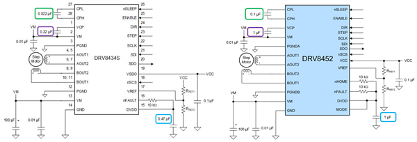
-
COMPONENT DRV8434S Recommended DRV8452 Recommended CVCP X7R, 0.22 uF, 16 V capacitor X7R, 1 uF, 16 V capacitor CSW X7R, 0.022 uF, VM-rated capacitor X7R, 0.1 uF, VM-rated capacitor CDVDD X7R, 0.47 uF to 1uF, 6.3 V capacitor X7R, 1 uF 6.3 V ceramic capacitor
- Off-Time PWM Chopping: The values of the time for Off-Time PWM chopping are slightly different between the two devices. See table below
-
TOFF state DRV8434S DRV8452 UNIT TOFF = 00b 7 9 μs TOFF = 01b
16 19 μs TOFF = 10b 24 27 μs TOFF = 11b 32 35 μs
-
- Decay Mode: Three decay modes are unavailable in DRV8452 as shown in the table below.
-
DECAY bits [2:0] DRV8434S DRV8452 000b Increasing SLOW, decreasing SLOW Slow decay 001b Increasing SLOW, decreasing MIXED 30% Reserved 010b Increasing SLOW, decreasing MIXED 60% Reserved 011b Increasing SLOW, decreasing FAST Reserved 100b Increasing MIXED 30%, decreasing MIXED 30% Mixed 30% decay 101b Increasing MIXED 60%, decreasing MIXED 60% Mixed 60% decay 110b Smart tune Dynamic Decay Smart tune Dynamic Decay 111b Smart tune Ripple Control Smart tune Ripple Control
-
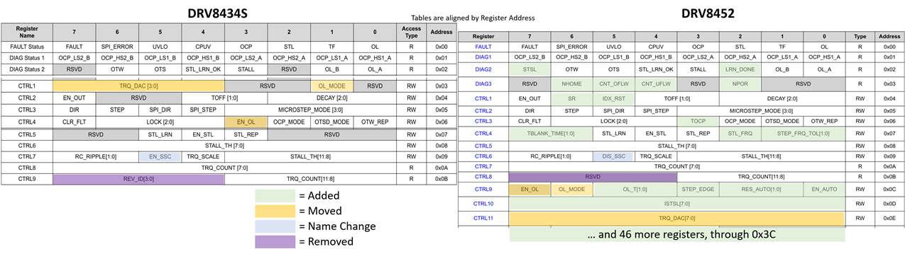
- Register Map: Many registers have been added and some register fields have been moved or renamed. See the table below for an illustration of the changes.
- Register fields moved:
- TRQ_DAC: Moved from Register Address 0x03 to 0x0E and was expanded from 4-bits to 8-bits.
- OL_MODE: Moved from Register Address 0x03 to 0x0C and moved bitfield from 1 to 6.
- EN_OL: Moved from Register Address 0x06 to 0x0C and moved bitfield from 3 to 7.
- Register fields removed:
- REV_ID
- Register fiends renamed:
- EN_SSC has changed to DIS_SSC. The functionality of this bit has also flipped. In DRV8434S, setting this bit = 1 results in Spread-Spectrum Enabled, whereas in DRV8452 this bit = 1 results in Spread-Spectrum Disabled.
- Note that the Register Name has changed for most registers, due to register 0x03 being renamed from "CTRL1" in DRV8434S to "DIAG3" in DRV8452. This resulted in all the CTRL# being decremented by 1 - CTRL2 renamed to CTRL1, CTRL3 renamed to CTRL2, etc. From a programming perspective since the Register Address didn't change this won't require any extensive firmware fixes.
- Register fields moved:
