This thread has been locked.

If you have a related question, please click the "Ask a related question" button in the top right corner. The newly created question will be automatically linked to this question.

DRV8316C-Q1: The GAIN/MODE/OCP/SLEW pin voltage is abnormal after power-on.

Part Number: DRV8316C-Q1
Other Parts Discussed in Thread: DRV8316,

Hi Team,

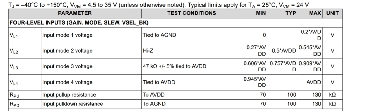
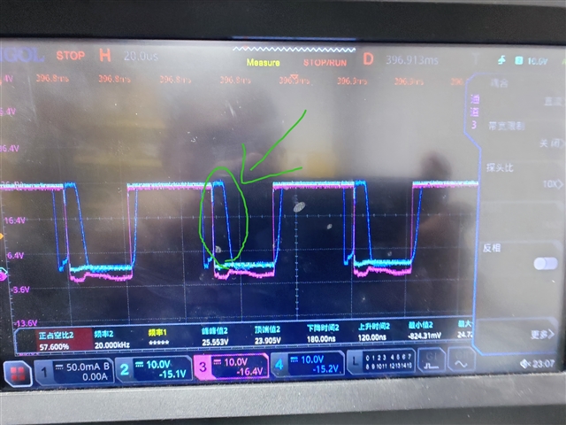
After DRV8316CT-Q1 is powered on, AVDD can output 3.3V normally, but the configuration pins GAIN/MODE/OCP/SLEW are not pulled up. If the pull-down resistor is not attached, it will be around 0.2V. If only 47KΩ pull-up is attached, the voltage will be 3.3V. If only 47KΩ pull-down is attached, the voltage will be 0V, and the remaining pin configurations will be normal.

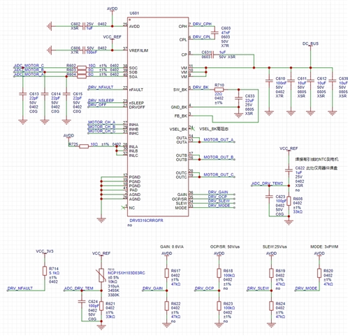
Pin configuration diagram:

Regards,

Annie

  • Hi Annie, 

    Is AVDD (3.3V) constant during these observations?  Can you take measurements of the voltage at the AVDD node, then across the resistors used, and then the voltage on the specific pin to further narrow down the source of this behavior?

    And can you also clarify what you mean here:

    If only 47KΩ pull-down is attached, the voltage will be 0V, and the remaining pin configurations will be normal.

    What do you mean by the remaining pin configurations will be normal?

    Best Regards,

    -Joshua

  • Hi Joshua,

    Yes, AVDD is constant 3.3VThe voltages at both ends of the resistor are the same, both at 3.3V or 0V. The pin voltage is consistent with the resistor voltage. nSLEEP voltage is 3.3V, NFAULT voltage is 3.3V, and DRVOFF voltage is 0V.

    Regards,

    Annie

  • Hi Annie,

    Thanks for the response.  

    I may be misunderstanding the issue so please correct me: 

    On the hardware settings pins (gain/slew/etc) when there is a resistor to select the mode, the voltage seen on the pin/47kOhm resistor (or 100kOhm pull-up/pull-down) is not accurate to what the datasheet says the device should see?  (Datasheet image below)

    Is this correct?

    Best Regards,

    -Joshua

  • Yes, you are correct.

    pull-up 47K is supposed to be 0.75*AVDD, actually it is AVDD. The levels of the MODE GAIN SLEW OCP configuration pins are incorrect.

    Regards,

    Annie

  • Hi Joshua,

    MODE forcibly configures the voltage to 0.75*AVDD by connecting an external pull-up resistor of 47k and a pull-down resistor of 150k. 

    At this time, DRV is connected to the three-phase motor and sends PWM waves to the three INHx channels. After sending 0.6s, DRV8316 is not working. He can see the OUTx pin of DRV no longer outputs the PWM wave, and SOx maintains Vref/2 and does not change. Tightening the motor by hand no longer produces a damping sensation. The customer suspected that the MOS tube inside the DRV8316 was completely disconnected at this time. nFAULT does not report an error. Repowering on and off through nSLEEP can solve the problem, but the three-phase motor has never been driven. 

    The OUTx waveform of DRV8316 is shown in the figure below, where CH2 is OUTA, CH3 is OUTB, and CH4 is OUTC. OUTA\B operates normally according to INHA\B, but OUTC is forcibly pulled high when it is low. He suspected that this was related to the abnormal opening and closing of the MOS tube in the DRV. After this phenomenon continues for a period of time, DRV8316 hangs up.

    Regards,

    Annie

  • Hi Joshua,

    In what scenario will the switch in the picture be turned off?

    Ragards,

    Annie

  • Hi Annie, 

    For MODE/GAIN/SLEW/OCP pins does increasing the pullup from 47K to 100K have any affect on the pin voltage? I am still a bit confused how the resistor is not decreasing the voltage seen on the pin and MODE still sees 3.3V instead of any decreased value. 

    Regarding the issue of OUTC, can you provide waveforms of the switch node (GHx, SHx) along with the inputs (INH/Lx) during this behavior? 

    And Lastly, if another DRV8316C-Q1 is available can you conduct an A-B-A swap to determine is this is an error/failure of this unit, or if we can narrow down the source to other external factors? For the Gate to go HIGH like this on only phase-C there might be a short in the phase-C switch node of the device. 

    Best Regards,

    -Joshua